LM4953中文资料

LM4953
Ground-Referenced,Ultra Low Noise,Ceramic Speaker Driver
General Description
The LM4953is an audio power amplifier designed for driving Ceramic Speaker in portable applications.When powered by a 3.6V supply,it is capable of forcing 12.6Vpp across a 2μF +30?bridge-tied-load (BTL)with less than 1%THD+N.Boomer audio power amplifiers were designed specifically to provide high quality output power with a minimal amount of external components.The LM4953does not require boot-strap capacitors,or snubber circuits.Therefore it is ideally suited for display applications requiring high power and mini-mal size.
The LM4953features a low-power consumption shutdown mode.Additionally,the LM4953features an internal thermal shutdown protection mechanism.
The LM4953contains advanced pop &click circuitry that eliminates noises which would otherwise occur during turn-on and turn-off transitions.
The LM4953is unity-gain stable and can be configured by external gain-setting resistors.
Key Specifications
j Quiescent Power Supply Current (V dd =3V)7mA(typ)j BTL Voltage Swing
(2μF+30?load,1%THD+N,V dd =3.6V)
12.6V pp (typ)j Shutdown Current
1μA (max)
Features
n Pop &click circuitry eliminates noise during turn-on and turn-off transitions
n Low,1μA (max)shutdown current n Low,7mA (typ)quiescent current
n 12.6Vpp mono BTL output,load =2μF+30?n Thermal shutdown n Unity-gain stable
n External gain configuration capability
Applications
n Cellphone n PDA
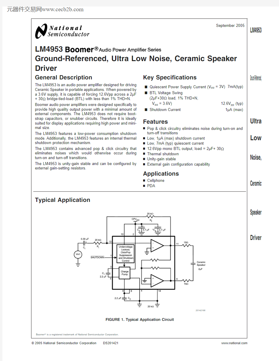
Typical Application
Boomer ?is a registered trademark of National Semiconductor Corporation.
20142168
FIGURE 1.Typical Application Circuit
September 2005
LM4953Ground-Referenced,Ultra Low Noise,Ceramic Speaker Driver
?2005National Semiconductor Corporation https://www.wendangku.net/doc/0a877663.html,
Connection Diagram
LLP Package
20142101
Top View
Order Number LM4953SD
See NS Package Number SDA14A
Pin Descriptions
Pin Name Function
1SD Active Low Shutdown 2CP VDD Charge Pump Power Supply
3CCP+Positive Terminal -Charge Pump Flying Capacitor 4PGND Power Ground
5CCP-Negative Terminal -Charge Pump Flying Capacitor 6V CP_OUT Charge Pump Output 7NC No Connect
8AV SS Negative Power Supply -Amplifier 9OUT B Output B
10AV DD Positive Power Supply -Amplifier 11OUT A Output A 12NC No Connect 13V IN Signal Input 14
SGND
Signal Ground
L M 4953
https://www.wendangku.net/doc/0a877663.html, 2
Absolute Maximum Ratings(Notes1,2) If Military/Aerospace specified devices are required, please contact the National Semiconductor Sales Office/ Distributors for availability and specifications.
Supply Voltage(V DD) 4.5V Storage Temperature?65?C to+150?C Input Voltage-0.3V to V DD+0.3V Power Dissipation(Note3)Internally Limited ESD Susceptibility(Note4)2000V ESD Susceptibility(Note5)200V
Junction Temperature150?C Thermal Resistance
See AN-1187’Leadless Leadframe Packaging(LLP).’
Operating Ratings
Temperature Range
T MIN≤T A≤T MAX?40?C≤T A≤85?C Supply Voltage(V DD) 1.6V≤V DD≤4.2V
Electrical Characteristics V
DD
=3.6V
The following specifications apply for V DD=3.6V,A V-BTL=6dB,Z L=2μF+30?unless otherwise specified.Limits apply to T A= 25?C.See Figure1.
Symbol Parameter Conditions LM4953Units(Limits)
Typ (Note6)
Limit (Notes7,8)
I DD Quiescent Power Supply
Current
V IN=0,R LOAD=2μF+30?8TBD mA(max)
I standby Quiescent Power Supply
Current Auto Standby Mode
V IN=0,Z LOAD=2μF+30? 2.7mA
I SD Shutdown Current V SD=GND0.11μA(max)
V SDIH Shutdown Voltage Input High SD1
SD2
0.7*CPVdd
V(min)
V SDIL Shutdown Voltage Input Low SD1
SD2
0.3*CPVdd
V(max)
T WU Wake-up Time125μsec
V OS Output Offset Voltage110mV(max)
V OUT Output Voltage Swing THD=1%(max);f=1kHz
R L=2μF+30?,Mono BTL
12.6Vpp
THD+N Total Harmonic Distortion+
Noise
V OUT=6Vp-p,f IN=1kHz0.02%
∈OS Output Noise A-Weighted Filter,V IN=0V15μV
PSRR Power Supply Rejection
Ratio
V RIPPLE=200mVp-p,f=217Hz,
Input Referred
67dB
V RIPPLE=200mVp-p,f=1kHz,
Input Referred
65dB
SNR Signal-to-Noise Ratio Z L=2μF+30?,V OUT=6Vp-p105dB
Electrical Characteristics V
DD
=3.0V
The following specifications apply for V DD=3.0V,A V-BTL=6dB,Z L=2μF+30?unless otherwise specified.Limits apply to T A= 25?C.See Figure1.
Symbol Parameter Conditions LM4953Units(Limits)
Typ (Note6)
Limit (Notes7,8)
I DD Quiescent Power Supply
Current
V IN=0,Z LOAD=2μF+30?710mA(max)
I standby Quiescent Power Supply
Current Auto Standby Mode
V IN=0,Z LOAD=2μF+30? 2.3mA
I SD Shutdown Current V SD-LC=V SD-RC=GND0.11μA(max)
V SDIH Shutdown Voltage Input High SD1
SD2
0.7*CPVdd
V(min)
LM4953
https://www.wendangku.net/doc/0a877663.html,
3
Electrical Characteristics V DD =3.0V
(Continued)
The following specifications apply for V DD =3.0V,A V-BTL =6dB,Z L =2μF+30?unless otherwise specified.Limits apply to T A =
25?C.See Figure 1.Symbol
Parameter
Conditions
LM4953
Units (Limits)
Typ (Note 6)
Limit (Notes 7,8)V SDIL Shutdown Voltage Input Low SD1SD2
0.3*CPVdd
V (max)T WU Wake-up Time 125μsec V OS Output Offset Voltage 1
10
mV (max)V OUT Output Voltage Swing THD =1%(max);f =1kHz Z L =2μF+30?,Mono BTL 10.2Vpp THD+N Total Harmonic Distortion +Noise V OUT =8.5Vp-p,f IN =1kHz 0.02%∈OS
Output Noise
A-Weighted Filter,V IN =0V 15μV PSRR
Power Supply Rejection Ratio
V RIPPLE =200mVp-p,f =217Hz,Input Referred
73dB V RIPPLE =200mVp-p,f =1kHz,Input Referred
68dB SNR
Signal-to-Noise Ratio
Z L =2μF+30?,V OUT =8.5Vp-p
105
dB Note 1:All voltages are measured with respect to the GND pin unless otherwise specified.
Note 2:Absolute Maximum Ratings indicate limits beyond which damage to the device may occur.Operating Ratings indicate conditions for which the device is functional but do not guarantee specific performance limits.Electrical Characteristics state DC and AC electrical specifications under particular test conditions that guarantee specific performance limits.This assumes that the device is within the Operating Ratings.Specifications are not guaranteed for parameters where no limit is given;however,the typical value is a good indication of device performance.
Note 3:The maximum power dissipation must be derated at elevated temperatures and is dictated by T JMAX ,θJA ,and the ambient temperature,T A .The maximum allowable power dissipation is P DMAX =(T JMAX –T A )/θJA or the number given in Absolute Maximum Ratings,whichever is lower.For the LM4xxx typical application (shown in Figure 1)with V DD =yyV,R L =2μF+30?mono BTL operation the total power dissipation is xxxW.θJA =40?C/W.Note 4:Human body model,100pF discharged through a 1.5k ?resistor.Note 5:Machine Model,220pF-240pF discharged through all pins.Note 6:Typicals are measured at 25?C and represent the parametric norm.
Note 7:Limits are guaranteed to National’s AOQL (Average Outgoing Quality Level).
Note 8:Datasheet min/max specification limits are guaranteed by design,test,or statistical analysis.
Note 9:If the product is in shutdown mode and V DD exceeds 3.6V (to a max of 4V V DD ),then most of the excess current will flow through the ESD protection circuits.If the source impedance limits the current to a max of 10mA,then the part will be protected.If the part is enabled when V DD is above 4V,circuit performance will be curtailed or the part may be permanently damaged.
L M 4953
https://www.wendangku.net/doc/0a877663.html, 4
Typical Performance Characteristics
THD+N vs Frequency
V DD=2V,V O=2Vpp,Z L=2μF+30?
THD+N vs Frequency
V DD=3V,V O=6Vpp,Z L=2μF+30?
2014211220142113
THD+N vs Frequency
V DD=3.6V,V O=8.5Vpp,Z L=2μF+30?
THD+N vs Frequency
V DD=4.2V,V O=10Vpp,Z L=2μF+30?
2014211420142118
THD+N vs Output Voltage
V DD=2V,f=1kHz,Z L=2μF+30?
THD+N vs Output Voltage
V DD=3V,f=1kHz,Z L=2μF+30?
20142119
20142121
LM4953
https://www.wendangku.net/doc/0a877663.html,
5
Typical Performance Characteristics
(Continued)
THD+N vs Output Voltage
V DD =3.6V,f =1kHz,Z L =2μF+30?
THD+N vs Output Voltage
V DD =4.2V,f =1kHz,Z L =2μF+30?
2014212020142122
PSRR vs Frequency V DD =2V,Z L =2μF+30?PSRR vs Frequency V DD =3V,Z L =2μF+30?
2014212320142125
PSRR vs Frequency V DD =3.6V,Z L =2μF+30?PSRR vs Frequency V DD =4.2V,Z L =2μF+30?
2014212420142126
L M 4953
https://www.wendangku.net/doc/0a877663.html, 6
Typical Performance Characteristics(Continued) Supply Current vs Supply Voltage
Z L=2μF+30?
20142127
Application Information
ELIMINATING THE OUTPUT COUPLING CAPACITOR The LM4953features a low noise inverting charge pump that generates an internal negative supply voltage.This allows the outputs of the LM4953to be biased about GND instead of a nominal DC voltage,like traditional headphone amplifi-ers.Because there is no DC component,the large DC blocking capacitors(typically220μF)are not necessary.The coupling capacitors are replaced by two,small ceramic charge pump capacitors,saving board space and cost. Eliminating the output coupling capacitors also improves low frequency response.In traditional headphone amplifiers,the headphone impedance and the output capacitor form a high pass filter that not only blocks the DC component of the output,but also attenuates low frequencies,impacting the bass response.Because the LM4953does not require the output coupling capacitors,the low frequency response of the device is not degraded by external components.
In addition to eliminating the output coupling capacitors,the ground referenced output nearly doubles the available dy-namic range of the LM4953when compared to a traditional headphone amplifier operating from the same supply volt-age.
BRIDGE CONFIGURATION EXPLANATION
The Audio Amplifier portion of the LM4953has two internal amplifiers allowing different amplifier configurations.The first amplifier’s gain is externally configurable,whereas the sec-ond amplifier is internally fixed in a unity-gain,inverting configuration.The closed-loop gain of the first amplifier is set by selecting the ratio of Rf to Ri while the second amplifier’s gain is fixed by the two internal20k?resistors.Figure1 shows that the output of amplifier one serves as the input to amplifier two.This results in both amplifiers producing sig-nals identical in magnitude,but out of phase by180?.Con-sequently,the differential gain for the Audio Amplifier is
A VD=2*(Rf/Ri)
By driving the load differentially through outputs OUT A and
OUT B,an amplifier configuration commonly referred to as
“bridged mode”is established.Bridged mode operation is
different from the classic single-ended amplifier configura-
tion where one side of the load is connected to ground.
A bridge amplifier design has a few distinct advantages over
the single-ended configuration.It provides differential drive
to the load,thus doubling the output swing for a specified
supply voltage.Four times the output power is possible as
compared to a single-ended amplifier under the same con-
ditions.This increase in attainable output power assumes
that the amplifier is not current limited or clipped.In order to
choose an amplifier’s closed-loop gain without causing ex-
cessive clipping,please refer to the Audio Power Amplifier
Design section.
The bridge configuration also creates a second advantage
over single-ended amplifiers.Since the differential outputs,
OUT A and OUT B,are biased at half-supply,no net DC
voltage exists across the load.This eliminates the need for
an output coupling capacitor which is required in a single
supply,single-ended amplifier configuration.Without an out-
put coupling capacitor,the half-supply bias across the load
would result in both increased internal IC power dissipation
and also possible loudspeaker damage.
OUTPUT TRANSIENT(’CLICK AND POPS’)
ELIMINATED
The LM4953contains advanced circuitry that virtually elimi-
nates output transients(’clicks and pops’).This circuitry
prevents all traces of transients when the supply voltage is
first applied or when the part resumes operation after coming
out of shutdown mode.
POWER DISSIPATION
Power dissipation is a major concern when using any power
amplifier and must be thoroughly understood to ensure a
successful design.Equation1states the maximum power
dissipation point for a single-ended amplifier operating at a
given supply voltage and driving a specified output load.
P DMAX=(V DD)2/(2π2Z L)(1)
LM4953
https://www.wendangku.net/doc/0a877663.html,
7
Application Information
(Continued)
Since the LM4953has two operational amplifiers in one package,the maximum internal power dissipation point is twice that of the number which results from Equation 1.Even with large internal power dissipation,the LM4953does not require heat sinking over a large range of ambient tempera-tures.The maximum power dissipation point obtained must not be greater than the power dissipation that results from Equation 2:
P DMAX =(T JMAX -T A )/(θJA )
(2)
Depending on the ambient temperature,T A ,of the system surroundings,Equation 2can be used to find the maximum internal power dissipation supported by the IC packaging.If the result of Equation 1is greater than that of Equation 2,then either the supply voltage must be decreased,the load impedance increased or T A reduced.Power dissipation is a function of output power and thus,if typical operation is not around the maximum power dissipation point,the ambient temperature may be increased accordingly.
POWER SUPPLY BYPASSING
As with any power amplifier,proper supply bypassing is critical for low noise performance and high power supply rejection.Applications that employ a 3V power supply typi-cally use a 4.7μF capacitor in parallel with a 0.1μF ceramic filter capacitor to stabilize the power supply’s output,reduce noise on the supply line,and improve the supply’s transient response.Keep the length of leads and traces that connect capacitors between the LM4953’s power supply pin and ground as short as possible.
AUTOMATIC STANDBY MODE
The LM4953features Automatic Standby Mode circuitry (patent pending).In the absence of an input signal,after approximately 3seconds,the LM4953goes into low current standby mode.The LM4953recovers into full power operat-ing mode immediately after a signal,which is greater than the input threshold voltage,is applied to either the left or right input pins.The input threshold voltage is not a static value,as the supply voltage increases,the input threshold voltage decreases.This feature reduces power supply current con-sumption in battery operated applications.
To ensure correct operation of Automatic Standby Mode,proper layout techniques should be implemented.Separat-ing PGND and SGND can help reduce noise entering the LM4953in noisy environments.It is also important to use correct power off sequencing.The device should be in shut-down and then powered off in order to ensure proper func-tionality of the Auto-Standby feature.While Automatic Standby Mode reduces power consumption very effectively during silent periods,maximum power saving is achieved by putting the device into shutdown when it is not in use.MICRO POWER SHUTDOWN
The voltage applied to the SD controls the LM4953’s shut-down function.When active,the LM4953’s micropower shut-down feature turns off the amplifiers’bias circuitry,reducing the supply current.The trigger point is 0.3*CPV DD for a logic-low level,and 0.7*CPV DD for logic-high level.The low 0.01μA (typ)shutdown current is achieved by applying a voltage that is as near as ground a possible to the SD pins.A voltage that is higher than ground may increase the shut-down current.
There are a few ways to control the micro-power shutdown.These include using a single-pole,single-throw switch,a microprocessor,or a microcontroller.When using a switch,connect an external 100k ?pull-up resistor between the SD pins and V DD .Connect the switch between the SD pins and ground.Select normal amplifier operation by opening the switch.Closing the switch connects the SD pins to ground,activating micro-power shutdown.The switch and resistor guarantee that the SD pins will not float.This prevents unwanted state changes.In a system with a microprocessor or microcontroller,use a digital output to apply the control voltage to the SD pins.Driving the SD pins with active circuitry eliminates the pull-up resistor.
SELECTING PROPER EXTERNAL COMPONENTS
Optimizing the LM4953’s performance requires properly se-lecting external components.Though the LM4953operates well when using external components with wide tolerances,best performance is achieved by optimizing component val-ues.
Charge Pump Capacitor Selection
Use low ESR (equivalent series resistance)(<100m ?)ce-ramic capacitors with an X7R dielectric for best perfor-mance.Low ESR capacitors keep the charge pump output impedance to a minimum,extending the headroom on the negative supply.Higher ESR capacitors result in reduced output power from the audio amplifiers.
Charge pump load regulation and output impedance are affected by the value of the flying capacitor (C1).A larger valued C1(up to 3.3uF)improves load regulation and mini-mizes charge pump output resistance.Beyond 3.3uF,the switch-on resistance dominates the output impedance for capacitor values above 2.2uF.
The output ripple is affected by the value and ESR of the output capacitor (C2).Larger capacitors reduce output ripple on the negative power supply.Lower ESR capacitors mini-mize the output ripple and reduce the output impedance of the charge pump.
The LM4953charge pump design is optimized for 2.2uF,low ESR,ceramic,flying,and output capacitors.
Input Capacitor Value Selection
Amplifying the lowest audio frequencies requires high value input coupling capacitors (C i in Figure 1).A high value ca-pacitor can be expensive and may compromise space effi-ciency in portable designs.In many cases,however,the speakers used in portable systems,whether internal or ex-ternal,have little ability to reproduce signals below 150Hz.Applications using speakers with this limited frequency re-sponse reap little improvement by using high value input and output capacitors.
Besides affecting system cost and size,C i has an effect on the LM4953’s click and pop performance.The magnitude of the pop is directly proportional to the input capacitor’s size.Thus,pops can be minimized by selecting an input capacitor value that is no higher than necessary to meet the desired ?3dB frequency.
As shown in Figure 1,the internal input resistor,R i and the input capacitor,C i ,produce a -3dB high pass filter cutoff frequency that is found using Equation (3).Conventional headphone amplifiers require output capacitors;Equation (3)can be used,along with the value of R L ,to determine to-wards the value of output capacitor needed to produce a –3dB high pass filter cutoff frequency.
L M 4953
https://www.wendangku.net/doc/0a877663.html,
8
Application Information(Continued)
f i-3dB=1/2πR i C i(3) Also,careful consideration must be taken in selectin
g a certain type of capacitor to be used in the system.Different
types of capacitors(tantalum,electrolytic,ceramic)have
unique performance characteristics and may affect overall
system performance.(See the section entitled Charge Pump
Capacitor Selection.)
LM4953
https://www.wendangku.net/doc/0a877663.html,
9
Revision History
Rev Date Description
1.02/18/05Started D/S by copying LM4926
(DS201161).1.29/13/05Added the Typ Perf curves and
Application Info section.1.39/14/05Added more Typ Perf curves.First WEB release on the D/S.1.4
9/19/05
Fixed some typo,then re-released D/S to
the WEB.
L M 4953
https://www.wendangku.net/doc/0a877663.html, 10
Physical Dimensions
inches (millimeters)unless otherwise noted
LLP Package
Order Number LM4953SD NS Package Number SDA14A
National does not assume any responsibility for use of any circuitry described,no circuit patent licenses are implied and National reserves the right at any time without notice to change said circuitry and specifications.For the most current product information visit us at https://www.wendangku.net/doc/0a877663.html,.LIFE SUPPORT POLICY
NATIONAL’S PRODUCTS ARE NOT AUTHORIZED FOR USE AS CRITICAL COMPONENTS IN LIFE SUPPORT DEVICES OR SYSTEMS WITHOUT THE EXPRESS WRITTEN APPROVAL OF THE PRESIDENT AND GENERAL COUNSEL OF NATIONAL SEMICONDUCTOR CORPORATION.As used herein:
1.Life support devices or systems are devices or systems which,(a)are intended for surgical implant into the body,or (b)support or sustain life,and whose failure to perform when properly used in accordance with instructions for use provided in the labeling,can be reasonably expected to result in a significant injury to the user.
2.A critical component is any component of a life support device or system whose failure to perform can be reasonably expected to cause the failure of the life support device or system,or to affect its safety or effectiveness.
BANNED SUBSTANCE COMPLIANCE
National Semiconductor manufactures products and uses packing materials that meet the provisions of the Customer Products Stewardship Specification (CSP-9-111C2)and the Banned Substances and Materials of Interest Specification (CSP-9-111S2)and contain no ‘‘Banned Substances’’as defined in CSP-9-111S2.Leadfree products are RoHS compliant.
National Semiconductor Americas Customer Support Center
Email:new.feedback@https://www.wendangku.net/doc/0a877663.html, Tel:1-800-272-9959
National Semiconductor
Europe Customer Support Center
Fax:+49(0)180-5308586Email:europe.support@https://www.wendangku.net/doc/0a877663.html,
Deutsch Tel:+49(0)6995086208English Tel:+44(0)8702402171Fran?ais Tel:+33(0)141918790
National Semiconductor Asia Pacific Customer Support Center
Email:ap.support@https://www.wendangku.net/doc/0a877663.html,
National Semiconductor
Japan Customer Support Center Fax:81-3-5639-7507
Email:jpn.feedback@https://www.wendangku.net/doc/0a877663.html, Tel:81-3-5639-7560
https://www.wendangku.net/doc/0a877663.html,
LM4953Ground-Referenced,Ultra Low Noise,Ceramic Speaker Driver