NE76100M中文资料

PART NUMBER NE76100PACKAGE OUTLINE
00 (CHIP)SYMBOLS PARAMETERS AND CONDITIONS
UNITS MIN
TYP MAX NF OPT 1Noise Figure at V DS = 3 V, I D = 10 mA, f = 4 GHz dB 0.8 1.4
G A 1Associated Gain at V DS = 3 V, I D = 10 mA, f = 4 GHz dB 12.0P 1dB
Output Power at 1 dB Gain Compression Point, f = 4 GHz V DS = 3 V, I DS = 10 mA dBm 12.5V DS = 3 V, I DS = 30 mA dBm 15.0G 1dB
Gain at P 1dB , f = 4 GHz V DS = 3 V, I DS = 10 mA dB 11.5V DS = 3 V, I DS = 30 mA
dB 13.5I DSS Saturated Drain Current at V DS = 3 V, V GS = 0mA 3060100V P Pinch Off Voltage at V DS = 3 V, I D = 100 m A V -3.0-1.1-0.5g m Transconductance at V DS = 3 V, I D = 10 mA mS 2045I GSO Gate to Source Leak Current at V GS = -5 V μA 1.0
10R TH 2
Thermal Resistance
°C/W
190Notes:
1.RF performance is determined by packaging and testing 10 samples per wafer. Wafer rejection criteria for standard devices is 2 rejects for 10 samples.
2.Chip mounted on an infinite heat sink.
DESCRIPTION
NE76100 is a high performance gallium arsenide metal semi-conductor field effect transistor chip. Its low noise figure makes this device appropriate for use in the second or third stages of low noise amplifiers operating in the 1-12 GHz frequency range. The device is fabricated using ion implantation for improved RF and DC performance, reliability, and uniformity.The NE76100 is suitable for a wide variety of commercial and industrial applications.
NEC's stringent quality assurance and test procedures assure the highest reliability and performance.
GENERAL PURPOSE
GaAs MESFET
NE76100
FEATURES
?LOW NOISE FIGURE:
NF = 0.8 dB typical at f = 4 GHz ?HIGH ASSOCIATED GAIN:
G A = 12.0 dB typical at f = 4 GHz ?L G = 1.0 μm, W G = 400 μm
ELECTRICAL CHARACTERISTICS (T A = 25°C)
A s s o c i a t e d G a i n , G A (d
B )
O p t i m u m N o i s e F i g u r e , N F O P T (d B )
Frequency, f (GHz)
NOISE FIGURE & ASSOCIATED
GAIN vs. FREQUENCY V DS = 3 V, I DS = 10 mA
California Eastern Laboratories
1 10 20
43.532.521.51
0.50
Ga
NF
242118151296
30
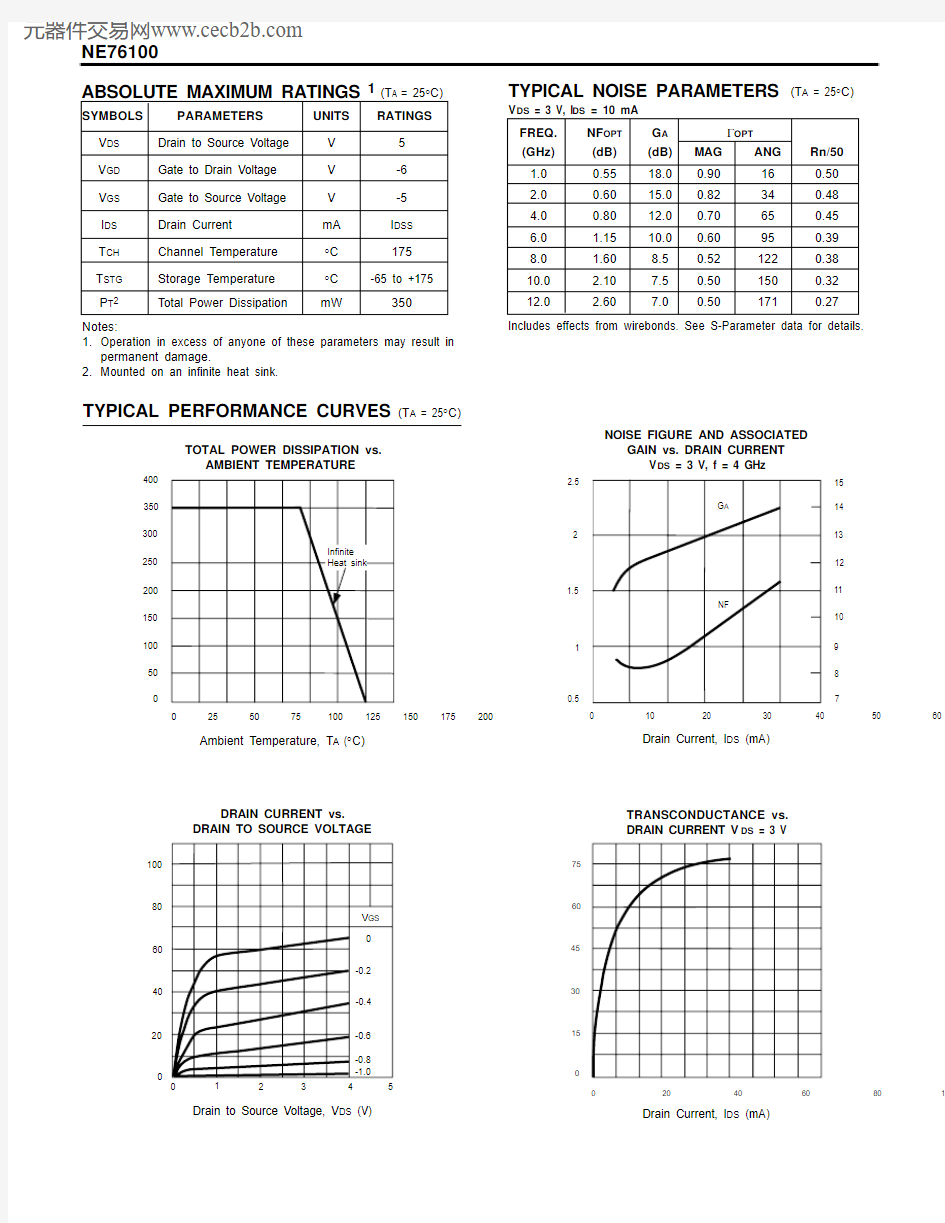
FREQ.NF OPT G AΓOPT
(GHz)(dB)(dB)MAG ANG Rn/50
1.00.5518.00.90160.50
2.00.6015.00.82340.48 4.00.8012.00.70650.45 6.0 1.1510.00.60950.39 8.0 1.608.50.521220.38
10.0 2.107.50.501500.32
12.0 2.607.00.501710.27
V GS
-0.2
-0.4
-0.6
-0.8
-1.0
01234
100
80
60
40
20
5
NE76100
ABSOLUTE MAXIMUM RATINGS1(T A = 25°C)
SYMBOLS PARAMETERS UNITS RATINGS
V DS Drain to Source Voltage V5
V GD Gate to Drain Voltage V-6
V GS Gate to Source Voltage V-5
I DS Drain Current mA I DSS
T CH Channel Temperature°C175
T STG Storage Temperature°C-65 to +175
P T2Total Power Dissipation mW350
T
o
t
a
l
P
o
w
e
r
D
i
s
s
i
p
a
t
i
o
n
,
P
T
(
m
W
)
T
r
a
n
s
c
o
n
d
u
c
t
a
n
c
e
,
g
m
(
m
S
)
A
s
s
o
c
i
a
t
e
d
G
a
i
n
,
G
A
(
d
B
)
N
o
i
s
e
F
i
g
u
r
e
,
N
F
(
d
B
)
Notes:
1.Operation in excess of anyone of these parameters may result in
permanent damage.
2.Mounted on an infinite heat sink.
TOTAL POWER DISSIPATION vs.
AMBIENT TEMPERATURE
D
r
a
i
n
C
u
r
r
e
n
t
,
I
D
S
(
m
A
)
DRAIN CURRENT vs.
DRAIN TO SOURCE VOLTAGE
TYPICAL PERFORMANCE CURVES(T A = 25°C)
Ambient Temperature, T A (°C)Drain Current, I DS (mA)
Drain Current, I DS (mA)
Includes effects from wirebonds. See S-Parameter data for details.
TYPICAL NOISE PARAMETERS (T A = 25°C)
V DS = 3 V, I DS = 10 mA
NOISE FIGURE AND ASSOCIATED
GAIN vs. DRAIN CURRENT
V DS = 3 V, f = 4 GHz
TRANSCONDUCTANCE vs.
DRAIN CURRENT V DS = 3 V
Drain to Source Voltage, V DS (V)
0 25 50 75 100 125 150 175 200
400
350
300
250
200
150
100
50
2.5
2
1.5
1
0.5
0 10 20 30 40 50 60
15
14
13
12
11
10
9
8
7
G A
NF
75
60
45
30
15
0 20 40 60 80 100
NE76100
FREQUENCY
S 11
S 21
S 12S 22
K
S 21MAG 1(GHz)MAG ANG MAG ANG MAG ANG MAG ANG (dB)(dB)0.10.99-2.3 3.782178.20.00486.70.769-1.20.05211.630.10.20.999-4.5 3.779176.30.00786.40.769-2.30.03711.527.10.50.996-11.3 3.763170.90.01883.10.767-5.70.04511.523.11.00.986-22.5 3.707161.90.03676.90.759-11.40.07611.218.41.50.971-33.3 3.619153.10.05370.80.74716.80.11011.420.12.00.951-43.9 3.505144.70.06865.00.731-22.00.14510.917.13.00.905-63.6 3.233128.90.09354.50.694-31.50.21410.215.44.00.859-81.4 2.941114.60.11245.50.657-39.70.2819.414.25.00.818-97.3 2.662101.90.12637.90.624-46.80.3478.513.36.00.784-111.4 2.41190.30.13531.50.598-53.10.4107.612.57.00.759 -124.2 2.19079.80.14126.10.577-58.90.470 6.811.98.00.739 -135.6 1.99970.10.14521.60.562-64.20.526 6.011.49.00.726-146.0 1.83361.10.14817.70.552-69.30.578 5.310.910.00.718-155.4 1.68852.70.14914.30.547-74.20.626 4.510.511.00.713-164.0 1.56244.70.14911.40.545-79.00.669 3.910.212.00.711-172.0 1.44937.20.1498.80.545-83.70.708 3.29.913.00.712-179.3 1.34929.90.148 6.70.548-88.30.741 2.69.614.00.715173.9 1.25923.00.147 4.80.554-92.90.770 2.09.315.00.719167.5 1.17716.40.146 3.20.561-97.50.793 1.49.116.00.725161.6 1.10210.00.144 1.80.569-102.1 0.8110.88.817.00.732156.1 1.033 3.80.1420.70.579-106.70.8240.38.618.00.739150.90.968-2.10.141-0.20.589-111.20.831-0.38.419.00.747146.00.908-7.80.139-0.90.601-115.70.833-0.88.120.0
0.755
141.4
0.851
-13.4
0.138
-1.5
0.613
-120.1
0.830-1.4
7.9
Note:
1.Gain Calculations:
MAG = Maximum Available Gain
MSG = Maximum Stable Gain
2.S-parameters include bond wires as follows:GATE:TOTAL 1 WIRE(S), 1 PER BOND PAD, 0.0134" (340 μm) LONG.DRAIN:TOTAL 2 WIRE(S), 1 PER BOND PAD, 0.0188" (477 μm) LONG.SOURCE:TOTAL 4 WIRE(S), 2 PER SIDE, 0.0114" (286 μm) LONG.WIRE:0.0007" (17.8 μm) DIA. GOLD.
TYPICAL SCATTERING PARAMETERS 2 (T A = 25°C)
V DS = 3 V, l DS = 10 mA
-j50
0?
+180–
MAG =
|S 21||S 12|
K - 1 ).2(K ±
? = S 11 S 22 - S 21 S 12
When K ≤ 1, MAG is undefined and MSG values are used.MSG =|S 21||S 12|, K = 1 + | ? | - |S 11| - |S 22|2222 |S 12 S 21|
,
NE76100
TYPICAL SCATTERING PARAMETERS 2 (T A = 25°C)
FREQUENCY
S 11S 21
S 12
S 22K S 21MAG 1(GHz)MAG ANG MAG ANG MAG ANG MAG ANG (dB)(dB)0.10.999
-2.5 4.692178.00.00386.50.713-1.20.05313.431.40.20.999-5.1 4.668176.10.00786.20.712-2.50.03813.428.40.50.995-12.7 4.662170.30.01782.70.710-6.20.04713.424.41.00.983-25.2
4.572160.70.03376.20.701-12.20.08113.221.41.50.965-37.3 4.435151.50.04869.80.686-17.90.11712.919.72.00.943-48.8 4.261142.60.06163.80.669-23.30.15412.618.43.00.893-70.1 3.860126.50.08353.30.629-33.00.22711.716.74.00.845-88.8 3.451112.30.09844.70.592-41.10.29910.81
5.45.00.805-105.2 3.07899.70.10937.80.560-48.00.3689.814.5
6.00.774-119.5 2.75488.60.11732.20.536-54.10.4348.813.7
7.00.752-132.1 2.4777
8.50.12227.70.519-5
9.60.4967.913.18.00.736-143.3 2.24269.20.12523.90.507-64.80.5547.012.59.00.726-153.3 2.04260.60.12720.80.500-69.80.606 6.212.010.00.720-162.3 1.87052.50.12918.20.497-74.70.654 5.411.611.00.717-170.6 1.72244.90.13016.10.497-79.40.696 4.711.212.00.717-178.1 1.59237.70.13114.20.500-84.20.732 4.010.913.00.719174.9 1.47730.70.13112.70.505-88.80.762 3.410.514.00.722168.5 1.37424.10.13111.40.511-93.50.787 2.810.215.00.727162.5 1.28217.70.13110.30.519-98.10.805 2.29.916.00.733156.9 1.19711.50.1319.40.529-102.70.816 1.69.617.00.739151.6 1.120 5.60.1318.60.539-107.20.823 1.09.318.00.746146.7 1.049-0.20.1317.90.551-111.70.8230.49.019.00.754142.10.983-5.70.1327.40.563-116.20.818-0.18.720.0
0.761
137.7
0.921
-11.1
0.132
6.9
0.575
-120.6
0.808
-0.7
8.4
Note:
1.Gain Calculations:
MAG = Maximum Available Gain
MSG = Maximum Stable Gain
2.S-parameters include bond wires as follows:GATE:TOTAL 1 WIRE(S), 1 PER BOND PAD, 0.0134" (340 μm) LONG.DRAIN:TOTAL 2 WIRE(S), 1 PER BOND PAD, 0.0188" (477 μm) LONG.SOURCE:TOTAL 4 WIRE(S), 2 PER SIDE, 0.0114" (286 μm) LONG.WIRE:0.0007" (17.8 μm) DIA. GOLD.
V DS = 3 V, l DS = 20 mA
-j50
?
+180–
MAG =
|S 21||S 12|
K - 1 ).2(K ±
? = S 11 S 22 - S 21 S 12
When K ≤ 1, MAG is undefined and MSG values are used.MSG =|S 21||S 12|, K = 1 + | ? | - |S 11| - |S 22|2222 |S 12 S 21|
,
FREQUENCY
S 11
S 21
S 12
S 22
K
S 21MAG 1(GHz)MAG ANG MAG ANG MAG ANG MAG ANG (dB)(dB)0.10.999-2.7 5.142178.00.00386.50.694-1.30.05414.232.00.20.999-5.4 5.137176.00.00686.10.693-2.50.03914.229.00.50.995-13.4 5.104169.90.01682.50.690-6.30.04914.225.01.00.982-26.6 4.995160.10.03175.70.680-12.50.08314.022.01.50.963-39.3 4.827150.60.04569.20.665-18.30.12013.720.32.00.939-51.4 4.619141.50.05863.20.647-23.70.15813.319.03.00.887-73.4 4.146125.20.07852.70.606-33.30.23312.417.34.00.840-92.5 3.676111.00.09244.40.569-41.20.30711.316.05.00.802-109.0 3.25698.60.10237.80.538-48.00.37810.315.16.00.773-123.3 2.89687.60.10832.60.516-53.90.4459.214.37.00.752-135.8 2.59477.60.11328.50.500-59.40.5088.313.68.00.738-146.8 2.34068.60.11625.10.490-64.50.5657.413.19.00.730-156.6 2.12560.10.11822.40.485-69.50.618 6.512.610.00.725-165.5 1.94152.20.12020.20.483-74.30.664 5.812.111.00.723-173.5 1.78344.70.12118.40.484-79.10.705 5.011.712.00.723179.1 1.64637.60.12216.80.487-83.80.739 4.311.313.00.726172.4 1.52430.80.12315.60.493-88.50.766 3.710.914.00.730166.1 1.41724.30.12414.50.500-93.20.787 3.010.615.00.735160.3 1.32018.00.12413.60.508-97.80.802 2.410.316.00.740154.8 1.23211.90.12512.90.518-102.50.810 1.89.917.00.747149.7 1.151 6.00.12612.20.529-107.00.812 1.29.618.00.754144.9 1.0770.40.12711.70.541-111.60.8080.69.319.00.761140.4 1.009-5.10.12811.20.553-116.10.8000.19.020.0
0.768
136.1
0.945
-10.4
0.129
10.8
0.566
-120.5
0.787-0.5
8.7
TYPICAL SCATTERING PARAMETERS 2 (T A = 25°C)
NE76100
Note:
1.Gain Calculations:
MAG = Maximum Available Gain
MSG = Maximum Stable Gain
2.S-parameters include bond wires as follows:GATE:TOTAL 1 WIRE(S), 1 PER BOND PAD, 0.0134" (340 μm) LONG.DRAIN:TOTAL 2 WIRE(S), 1 PER BOND PAD, 0.0188" (477 μm) LONG.SOURCE:TOTAL 4 WIRE(S), 2 PER SIDE, 0.0114" (286 μm) LONG.WIRE:0.0007" (17.8 μm) DIA. GOLD.
V DS = 3 V, l DS = 30 mA
MAG =
|S 21||S 12|
K - 1 ).2(K ±
? = S 11 S 22 - S 21 S 12
When K ≤ 1, MAG is undefined and MSG values are used.MSG =|S 21||S 12|, K = 1 + | ? | - |S 11| - |S 22|2222 |S 12 S 21|
,
-j50
0?
+180–
FREQUENCY
S 11
S 21
S 12
S 22
K
S 21MAG 1(GHz)MAG ANG MAG ANG MAG ANG MAG ANG (dB)(dB)0.10.999-2.8 5.433177.90.00386.40.685-1.30.05414.732.40.20.999-5.6 5.428175.90.00686.00.684-2.50.03914.729.40.50.995-13.9 5.391169.70.01582.30.681-6.30.04914.625.41.00.981-27.5 5.267159.60.03075.50.671-12.5
0.08514.422.41.50.961-40.6 5.079150.00.04469.00.655-18.30.12314.120.72.00.937-53.0 4.846140.80.05562.90.637-23.70.16213.719.43.00.885-75.5 4.325124.40.07452.60.596-33.10.239
12.717.74.00.838-94.8 3.815110.20.08744.40.559-40.80.31311.616.45.00.800-111.3 3.36597.80.09638.10.530-47.40.38510.515.46.00.773-125.6 2.98486.90.10233.20.508-53.20.4539.514.77.00.753-138.0 2.66677.10.10729.40.494-58.50.5168.514.08.00.741-148.9 2.40068.10.11026.30.484-63.60.5737.613.49.00.733-158.6 2.17659.80.11223.90.480-68.60.625 6.812.910.00.728-167.3 1.98551.90.11421.90.479-73.40.670 6.012.411.00.727-175.2 1.82144.50.11520.30.480-78.20.709 5.212.012.00.728177.6 1.67937.50.11718.90.484-82.90.740 4.511.613.00.731170.9 1.55430.70.11817.80.490-87.70.765 3.811.214.00.734164.7 1.44224.30.11916.90.497-92.40.784 3.210.815.00.739159.0 1.34318.00.12016.20.506-97.10.795 2.610.516.00.745153.6 1.25212.00.12115.50.516-101.70.800 2.010.117.00.751148.6 1.170 6.20.12314.90.527-106.30.799 1.49.818.00.758143.9 1.0940.50.12414.40.538-110.90.7930.89.519.00.765139.4 1.024-4.90.12513.90.551-115.40.7820.29.120.0
0.772
135.2
0.959
-10.2
0.127
13.5
0.563
-119.9
0.767-0.4
8.8
NE76100
TYPICAL SCATTERING PARAMETERS 2 (T A = 25°C)
Note:
1.Gain Calculations:
MAG = Maximum Available Gain
MSG = Maximum Stable Gain
2.S-parameters include bond wires as follows:GATE:TOTAL 1 WIRE(S), 1 PER BOND PAD, 0.0134" (340 μm) LONG.DRAIN:TOTAL 2 WIRE(S), 1 PER BOND PAD, 0.0188" (477 μm) LONG.SOURCE:TOTAL 4 WIRE(S), 2 PER SIDE, 0.0114" (286 μm) LONG.WIRE:0.0007" (17.8 μm) DIA. GOLD.
V DS = 3 V, l DS = 40 mA
-j50
?
+180–
MAG =
|S 21||S 12|
K - 1 ).2(K ±
? = S 11 S 22 - S 21 S 12
When K ≤ 1, MAG is undefined and MSG values are used.MSG =|S 21||S 12|, K = 1 + | ? | - |S 11| - |S 22|2222 |S 12 S 21|
,元器件交易网https://www.wendangku.net/doc/0b2679335.html,
NE76100
MODEL RANGE
Frequency:0.1 to 20 GHz
Bias:V DS = 3 V, I D = 10, 20, 30, 40 mA Date:
10/23/96
Parameter Units
capacitance picofarads inductance nanohenries resistance ohms
conductance millisiemans
time
picoseconds frequency
gigahertz
UNITS
SCHEMATIC
Parameters
3 V, 10 mA 3 V, 20 mA
3 V, 30 mA 3 V, 40 mA g 48 mS 63 mS 70 mS 76 mS t 5 pSec 4.5 pSec 4.5 pSec
4 pSec RDS 350 ohms 260 ohms 240 ohms 230 ohms CGS 0.4
5 pF 0.52 pF 0.57 pF 0.61pF CDG
0.07 pF
0.068 pF
0.065 pF
0.061 pF
BIAS DEPENDANT MODEL PARAMETERS
NE76100 LINEAR MODEL
SOURCE
元器件交易网https://www.wendangku.net/doc/0b2679335.html,
NE76100
PART NUMBER IDSS SELECTION NE7610030 to 100 mA (Standard)
NE76100N 30 to 60NE76100M
60 to 100
ORDERING INFORMATION
OUTLINE DIMENSIONS (Units in μm)
NE76100 (CHIP)
Chip Thickness: 140 μm
Note:
All dimensions are typical unless otherwise specified.
EXCLUSIVE NORTH AMERICAN AGENT FOR RF, MICROWAVE & OPTOELECTRONIC SEMICONDUCTORS
? Headquarters ? 4590 Patrick Henry Drive ? Santa Clara, CA 95054-1817 ? (408) 988-3500 ? Telex 34-6393 ? FAX (408) 988-0279
24-Hour Fax-On-Demand: 800-390-3232 (U.S. and Canada only) ? Internet: https://www.wendangku.net/doc/0b2679335.html,
12/02/99DATA SUBJECT TO CHANGE WITHOUT NOTICE
元器件交易网https://www.wendangku.net/doc/0b2679335.html,