NTF3055L175T1G中文资料

NTF3055L175
Preferred Device
Power MOSFET
2.0 A, 60 V , Logic Level
N?Channel SOT?223
Designed for low voltage, high speed switching applications in power supplies, converters and power motor controls and bridge circuits.
Features
?Pb?Free Packages are Available
Applications
?Power Supplies ?Converters
?Power Motor Controls ?
Bridge Circuits
MAXIMUM RATINGS (T
= 25°C unless otherwise noted)
0.995 in 2).
2.When surface mounted to an FR4 board using minimum recommended pad size, 2?2.4 oz. (Cu. Area 0.272 in 2).
https://www.wendangku.net/doc/068421798.html,
See detailed ordering and shipping information in the package dimensions section on page 5 of this data sheet.ORDERING INFORMATION
Preferred devices are recommended choices for future use and best overall value.
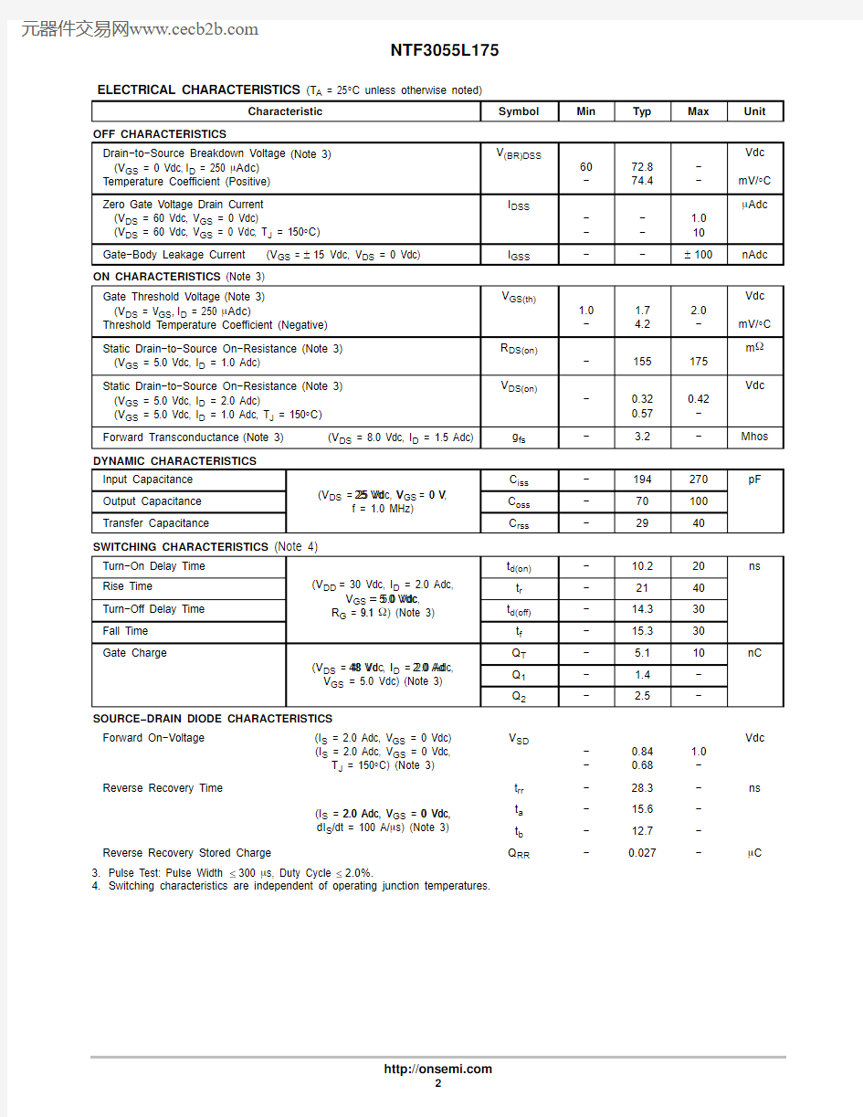
ELECTRICAL CHARACTERISTICS (T
= 25°C unless otherwise noted)
SWITCHING CHARACTERISTICS
4.Switching characteristics are independent of operating junction temperatures.
Figure 5. On?Resistance Variation with
Temperature
Figure 6. Drain?to?Source Leakage Current
versus Voltage
R D S (o n ), D R A I N ?T O ?S O U R C E R E S I S T A N C E (W )
T J , JUNCTION TEMPERATURE (°C)R D S (o n ), D R A I N ?T O ?S O U R C E R E S I S T A N C E (N O R M A L I Z E D )
?50
50250?2575125100150V DS, DRAIN?TO?SOURCE VOLTAGE (VOLTS)
I D , D R A I N C U R R E N T (A M P S )
175
10010.1
0.001
100
10
1
700500400C , C A P A C I T A N C E (p F )
300
200
S )
t , T I M E (n s )
Figure 11. Maximum Rated Forward Biased
Safe Operating Area V DS , DRAIN?TO?SOURCE VOLTAGE (VOLTS)Figure 12. Maximum Avalanche Energy versus
Starting Junction Temperature
T J , STARTING JUNCTION TEMPERATURE (°C)
I D , D R A I N C U R R E N T (A M P S )
0.010********
100
0.1
100
10
1
0.1
0.001
1000
r (t ), E F F E C T I V E T R A N S I E N T T H E R M A L R E S I S T A N C E (N O R M A L I Z E D )
t, TIME (s)
Figure 13. Thermal Response
10
1
0.01
0.0001
0.00001
ORDERING INFORMATION
Specifications Brochure, BRD8011/D.
PACKAGE DIMENSIONS
STYLE 3:PIN 1.
GATE 2.DRAIN 3.SOURCE 4.
DRAIN
DIM A MIN MAX MIN MAX MILLIMETERS 0.2490.263 6.30 6.70INCHES
B 0.1300.145 3.30 3.70
C 0.0600.068 1.50 1.75
D 0.0240.0350.600.89F 0.1150.126 2.90 3.20G 0.0870.094 2.20 2.40H 0.00080.00400.0200.100J 0.0090.0140.240.35K 0.0600.078 1.50 2.00L 0.0330.0410.85 1.05M 0 10 0 10 S 0.2640.287 6.707.30
NOTES:
1.DIMENSIONING AND TOLERANCING PER ANSI Y14.5M, 198
2.
2.CONTROLLING DIMENSION: INCH.
____SOT?223 (TO?261)CASE 318E?04
ISSUE K
*For additional information on our Pb?Free strategy and soldering
details, please download the ON Semiconductor Soldering and Mounting Techniques Reference Manual, SOLDERRM/D.
SOLDERING FOOTPRINT*
SOT?223
ON Semiconductor and are registered trademarks of Semiconductor Components Industries, LLC (SCILLC). SCILLC reserves the right to make changes without further notice to any products herein. SCILLC makes no warranty, representation or guarantee regarding the suitability of its products for any particular purpose, nor does SCILLC assume any liability arising out of the application or use of any product or circuit, and specifically disclaims any and all liability, including without limitation special, consequential or incidental damages.“Typical” parameters which may be provided in SCILLC data sheets and/or specifications can and do vary in different applications and actual performance may vary over time. All operating parameters, including “Typicals” must be validated for each customer application by customer’s technical experts. SCILLC does not convey any license under its patent rights nor the rights of others. SCILLC products are not designed, intended, or authorized for use as components in systems intended for surgical implant into the body, or other applications intended to support or sustain life, or for any other application in which the failure of the SCILLC product could create a situation where personal injury or death may occur. Should Buyer purchase or use SCILLC products for any such unintended or unauthorized application, Buyer shall indemnify and hold SCILLC and its officers, employees, subsidiaries, affiliates,and distributors harmless against all claims, costs, damages, and expenses, and reasonable attorney fees arising out of, directly or indirectly, any claim of personal injury or death associated with such unintended or unauthorized use, even if such claim alleges that SCILLC was negligent regarding the design or manufacture of the part. SCILLC is an Equal Opportunity/Affirmative Action Employer. This literature is subject to all applicable copyright laws and is not for resale in any manner.
PUBLICATION ORDERING INFORMATION