911+SMD911_D_DD0002_

S M D 911
FEATURES
DESCRIPTION
Operate from a rectified 85~265 VAC line source.
Typical oscillation frequency:90 kHz Unnecessary external DC Power supply Output voltage external setting (FB) type available.
FB terminal voltage (VFB) 1.0 V.
Duty ratio: 0% to 5% typ.-PFM control,5% to 85% typ.-PWM control
Built-in current limiting circuit: Assigned by external resistor.
Soft-start function: Built-in Soft-start circuit.
Built-in HV regulator.
The SMD911is a monolithic high voltage switching regulator-controller with PWM/PFM control that is specifically designed to operate from a rectified 85~265 VAC line source.
This device contains a reference voltage source,oscillation circuit, error amplifier, phase
compensation circuit, PWM control circuit, power supply 450 V MOS-transistor, and other
components. Since the oscillation frequency is at high 90 kHz,with the addition of a small external component, the IC can function as switching regulator with high efficiency.
The SMD911provides low-ripple power,high-efficiency, and excellent transient
characteristics because of the PWM control circuit being capable of varying the duty ratio from 0% to 85%linearly and the optimized error amplifier with the phase compensation circuit.
The SMD911contains PWM/PFM switching control circuit such that it operates in PWM mode at 5% or higher duty ratio and in PFM mode below 5% duty ratio to ensure high efficiency in all load ranges.
APPLICATIONS
LED Drivers
Back Lighting
Energy Saving Illumination
High Voltage Switching Regulator Non-Isolation Controller
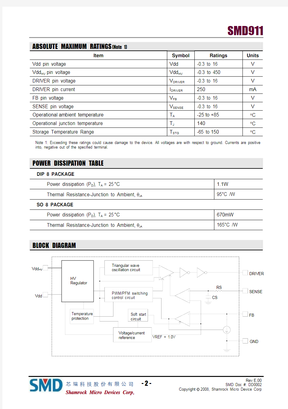
ABSOLUTE MAXIMUM RATINGS (Note 1)
Item
Symbol Ratings Units Vdd pin voltage Vdd -0.3 to 16V Vdd HV pin voltage Vdd HV -0.3 to 450V DRIVER pin voltage V DRIVER -0.3 to 16V DRIVER pin current I DRIVER 250mA FB pin voltage V FB -0.3 to 16V SENSE pin voltage
V
SENSE -0.3 to 16V Operational ambient temperature T A -25to +85°C Operational junction temperature T J 140°C Storage Temperature Range
T STG
-65 to 150
°C
Note 1: Exceeding these ratings could cause damage to the device. All voltages are with respect to ground. Currents are positive into, negative out of the specified terminal.
POWER DISSIPATION TABLE
DIP 8 PACKAGE
Power dissipation (P D ), T A = 25°C
1.1W Thermal Resistance-Junction to Ambient,θJA
95°C /W
SO 8 PACKAGE
Power dissipation (P D ), T A = 25°C
670mW Thermal Resistance-Junction to Ambient,θJA
165°C /W BLOCK DIAGRAM
FB
Vdd GND
DRIVER
SENSE
TYPICAL APPLICATIONS
Fig.1.85~265V AC input,12V/0.5A Output Buck
Converter
Fig.2.85~265V AC input,Buck-Boost constant current mode
When LED’s are opened, V OUT= 400V DC 12V GND
F1
LED +
-
ELECTRICAL CHARACTERISTICS Unless otherwise specified, T A=-25O C.~ 85O C; Vdd HV= 120V DC
Parameter Test Conditions Symbol Min Typ Max Units Output resistance at low level
output voltage
I OL= 20mA R OL 4.4 6.516?Output resistance at high
level output voltage
I OH=-20mA R OH131630?Minimum supply voltage V HVmin---2230V Current consumption in static
mode
I FB=0.25mA I CC10.30.61 1.0mA Current consumption without
load
I CC20.40.67 1.0mA Current consumption with
load
1nF Output Load on Pin 5I CC3 1.2 1.72 2.2mA Operating frequency f OSC8090100kHz Maximum duty ratio I FB=1uA d max778189% PWM/PFM switch duty ratio d min 5.0% Duty ratio I FB=0.1mA d01mA32% Maximum control current at
FB pin
Duty Cycle = 0 %I FBmax140200uA
FB pin voltage Switching Phase,
I FB=0.1mA(25°C)
V FB0.981 1.02V
FB pin voltage Switching Phase,
I FB=0.1mA
V FB0.96 1.04V
Load regulation I FB=0.02mA~0.25mA?V FB12540mV Input bias current Through Pin 1I B-CS-4.00 4.0uA Threshold at current detector
input
V CS-th0.90.98 1.05V
Output voltage fall time C DRIVER=1nF, from 90%
down to 10% of Output
Signal
t f---250ns
Output voltage rise time C DRIVER=1nF, from 10% up
to 90% of Output Signal
t r---250ns
Soft-start time From appearance pulses at
DRIVER pin to increase
Duty Cycle more 50%
t SS4915ms
Start voltage at Vdd pin Vstup12.213.013.4V Overvoltage protection
threshold
Vovp14.415.416V
On-voltage of high voltage
power supply
Vcc-on7.37.78.1V
Off-voltage of high voltage
power supply
Vcc-off7.68.08.4V Thermal Shutdown T OTP150°C
PACKAGE DESCRIPTION Dimensions in inches (millimeters) unless otherwise specified SO 8
DIP 8
0.100 +/- 0.010(2.540 +/- 0.254)
911M911MS YY = Year, WW = Working Week
IMPORTANT NOTICE
Shamrock Micro Devices(SMD) reserves the right to make changes to its products or to discontinue any integrated circuit product or service without notice, and advises its customers to obtain the latest version of relevant information to verify, before placing orders, that the information being relied on is current.
A few applications using integrated circuit products may involve potential risks of death, personal injury, or severe property or environmental damage. SMD integrated circuit products are not designed, intended, authorized, or warranted to be suitable for use in life-support applications, devices or systems or other critical applications. Use of SMD products in such applications is understood to be fully at the risk of the customer. In order to minimize risks associated with the customer’s applications, the customer should provide adequate design and operating safeguards.