A6832EEP-T中文资料

Data Sheet 26185.110E
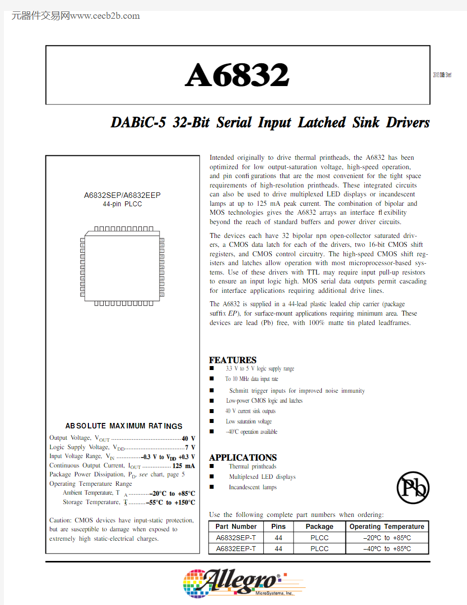
A6832
DABiC-5 32-Bit Serial Input Latched Sink Drivers
Intended originally to drive thermal printheads, the A6832 has been optimized for low output-saturation voltage, high-speed operation, and pin con ? gurations that are the most convenient for the tight space requirements of high-resolution printheads. These integrated circuits can also be used to drive multiplexed LED displays or incandescent lamps at up to 125 mA peak current. The combination of bipolar and MOS technologies gives the A6832 arrays an interface ? exibility beyond the reach of standard buffers and power driver circuits.The devices each have 32 bipolar npn open-collector saturated driv-ers, a CMOS data latch for each of the drivers, two 16-bit CMOS shift registers, and CMOS control circuitry. The high-speed CMOS shift reg-isters and latches allow operation with most microprocessor-based sys-tems. Use of these drivers with TTL may require input pull-up resistors to ensure an input logic high. MOS serial data outputs permit cascading for interface applications requiring additional drive lines.
The A6832 is supplied in a 44-lead plastic leaded chip carrier (package suf ? x EP ), for surface-mount applications requiring minimum area. These devices are lead (Pb) free, with 100% matte tin plated leadframes.
3.3 V to 5 V logic supply range To 10 MHz data input rate
Schmitt trigger inputs for improved noise immunity Low-power CMOS logic and latches 40 V current sink outputs Low saturation voltage –40°C operation available
Use the following complete part numbers when ordering:
Part Number Pins Package Operating Temperature
A6832SEP-T 44PLCC –20oC to +85oC A6832EEP-T
44
PLCC
–40oC to +85oC
FEATURES
Thermal printheads
Multiplexed LED displays Incandescent lamps
APPLICATIONS
DABiC-5 32-Bit Serial-Input Latched Sink Drivers
Functional Block Diagram
C LOC K S E R IAL DATA S TR OB E
OUTP UT E NAB
LE
V DD
S E R IAL DATA OUT
OUT OUT OUT OUT OUT OUT 123303132
G R OUND Typical Input Circuit
Typical Output Driver
DABiC-5 32-Bit Serial-Input Latched Sink Drivers
ELECTRICAL CHARACTERISTICS 1 Unless otherwise noted: T A = 25°C, logic supply operating voltage V dd =
3.0 V to 5.5 V
1Positive (negative) current is de ? ned as conventional current going into (coming out of) the speci ? ed device pin.2Operation at a clock frequency greater than the speci ? ed minimum value is possible but not warran teed.
L = Low Logic Level H = High Logic Level X = Irrelevant P = Present State R = Previous State
Truth Table
DABiC-5 32-Bit Serial-Input Latched Sink Drivers
Timing Requirements and Speci ? cations
(Logic Levels are V DD and Ground)
C LOC
S E R DATA S TR OUTP UT E NAB OUT S E R DATA OUTP UT E NAB LE
OUT N
DATA
10%
50%
dis(B Q)
t en(B Q)
t LOW =ALL OUTP UTS B LANK E D (DIS AB LE D)
r
t f
t 50%
90%NOTE: Timing is representative of a 10 MHz clock. Higher speeds may be attainable; operation at high temperatures will reduce the speci ? ed maximum clock frequency.
S erial Data present at the input is transferred to the shift register on the logical 0 to logical 1 transition of the CLOCK input pulse. On
succeeding CLOCK pulses, the registers shift data information towards the SERIAL DA TA OUTPUT. The SERIAL DA TA must appear at the input prior to the rising edge of the CLOCK input waveform.
Information present at any register is transferred to the respective latch when the STROBE is high (serial-to-parallel conversion). The
latches will continue to accept new data as long as the STROBE is held high. Applications where the latches are bypassed (STROBE tied high) will require that the OUTPUT ENABLE input be low during serial data entry.
When the OUTPUT ENABLE input is low, the output sink drivers are disabled (OFF). The information stored in the latches is not affected by the OUTPUT ENABLE input. With the OUTPUT
ENABLE input high, the outputs are controlled by the state of their respective latches.
Key Description
Symbol Time (ns)A Data Active Time Before Clock Pulse (Data Set-Up Time)t su(D)25B Data Active Time After Clock Pulse (Data Hold Time)t h(D)25C Clock Pulse Width
t w(CH)50D Time Between Clock Activation and Strobe t su(C)100E
Strobe Pulse Width
t w(STH)
50
O U T N C
S T R O B E
1
G R O U N D S E R I A L D A T A I N
L O G I C S U P P L Y C L O C K
S E R I A L D A T A O U T O U T P U T
E N A B L E
N C
O U T 3231OUT 21
N C O U T 1O U T 1I C O U T 1O U T 20N C 32
OUT 12OUT 2
A6832SEP/A6832EEP
5075100125150
AMBIENT TEMPERATURE (oC)
25
*Additional thermal information is available on the Allegro Web site.
DABiC-5 32-Bit Serial-Input Latched Sink Drivers
Dimensions in Inches
(controlling dimensions)
Dimensions in Millimeters (for reference only)18
Dwg. MA-005-44A in
Dwg. MA-005-44A mm NOTES: 1.Exact body and lead configuration at vendor’s option within limits shown.
2.Lead spacing tolerance is non-cumulative.
A6832SEP and A6832EEP
DABiC-5 32-Bit Serial-Input Latched Sink Drivers
The products described here are manufactured under one or
more U.S. patents or U.S. patents pending.
Allegro MicroSystems, Inc. reserves the right to make, from time
to time, such de p ar t ures from the detail spec i?c a t ions as may be
required to permit improvements in the per f or m ance, reliability,
or manufacturability of its products. Before placing an order, the
user is cautioned to verify that the information being relied upon is
current.
Allegro products are not authorized for use as critical compo-
nents in life-support devices or sys t ems without express written
approval.
The in f or m a t ion in c lud e d herein is believed to be ac c u r ate and
reliable. How e v e r, Allegro MicroSystems, Inc. assumes no re s pon -
si b il i t y for its use; nor for any in f ringe m ent of patents or other
rights of third parties which may result from its use.
Copyright?2003, 2004, 2005 AllegroMicrosystems, Inc.