KLM4GxxEHx (FN3x based moviNAND)_1.1
KLMXGXXEHX
Rev. 1.1, Nov. 2009SAMSUNG ELECTRONICS RESERVES THE RIGHT TO CHANGE PRODUCTS, INFORMATION AND SPECIFICATIONS WITHOUT NOTICE.
Products and specifications discussed herein are for reference purposes only. All information discussed herein is provided on an "AS IS" basis, without warranties of any kind.
This document and all information discussed herein remain the sole and exclusive property of Samsung Electronics. No license of any patent, copyright, mask work, trademark or any other intellectual property right is granted by one party to the other party under this document, by implication, estoppel or other-wise.
Samsung products are not intended for use in life support, critical care, medical, safety equipment, or similar applications where product failure could result in loss of life or personal or physical harm, or any military or defense application, or any governmental procurement to which special terms or provisions may apply.
For updates or additional information about Samsung products, contact your nearest Samsung office.All brand names, trademarks and registered trademarks belong to their respective owners.?2009 Samsung Electronics Co., Ltd. All rights reserved.
Samsung eMMC moviNAND Product family
eMMC Specification compatibility
datasheet
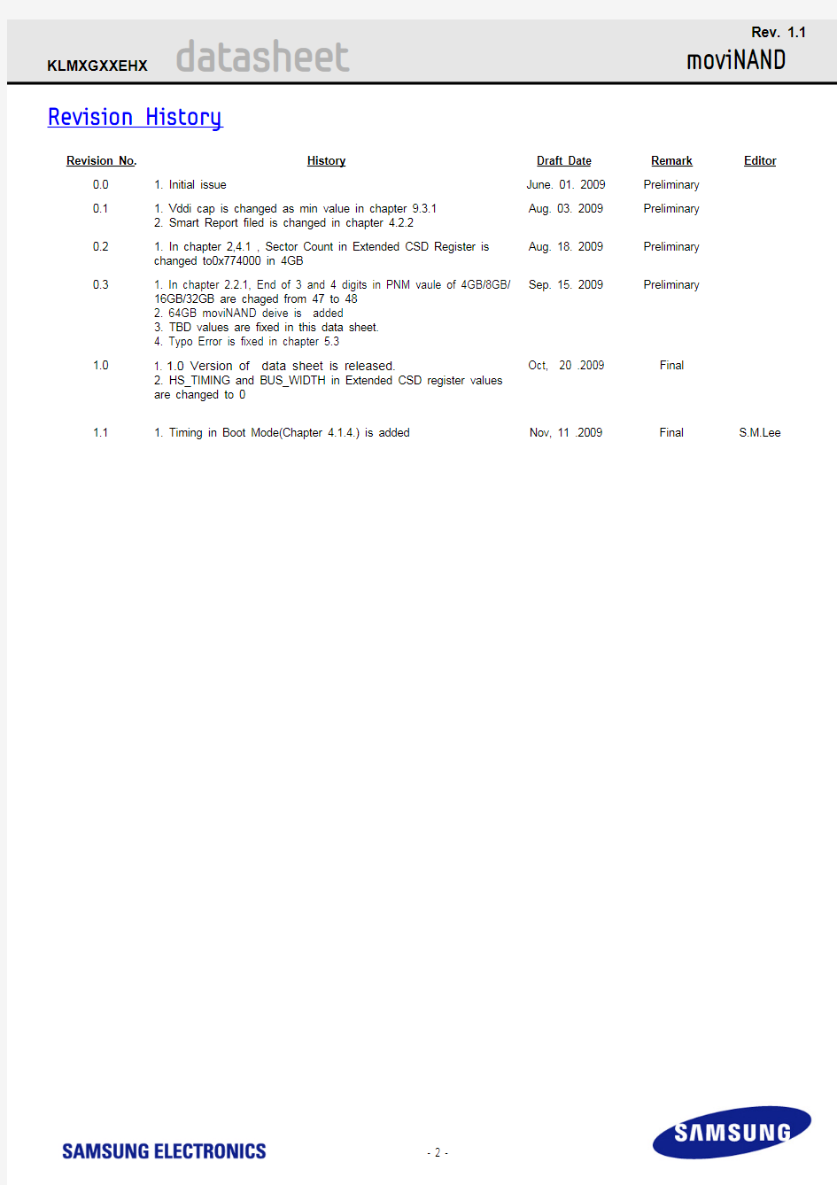
Revision History
Revision No.History Draft Date Remark Editor
0.0 1. Initial issue June. 01. 2009Preliminary
Aug. 03. 2009Preliminary
0.1 1. Vddi cap is changed as min value in chapter 9.3.1
2. Smart Report filed is changed in chapter 4.2.2
0.2 1. In chapter 2,4.1 , Sector Count in Extended CSD Register is
Aug. 18. 2009Preliminary
changed to0x774000 in 4GB
Sep. 15. 2009Preliminary
0.3 1. In chapter 2.2.1, End of 3 and 4 digits in PNM vaule of 4GB/8GB/
16GB/32GB are chaged from 47 to 48
2. 64GB moviNAND deive is added
3. TBD values are fixed in this data sheet.
4. Typo Error is fixed in chapter
5.3
Oct, 20 .2009Final
1.0 1. 1.0 Version of data sheet is released.
2. HS_TIMING and BUS_WIDTH in Extended CSD register values
are changed to 0
1.1 1. Timing in Boot Mode(Chapter 4.1.4.) is added Nov, 11 .2009Final S.M.Lee
Table Of Contents
1.0 Product List (4)
2.0 Key Features (4)
3.0 Package Configurations (5)
3.1 Pin Configuration (5)
3.2 Package Dimensions (6)
3.3 Product Architecture (7)
4.0 Features of moviNAND (8)
4.1 Vendor specific command (8)
4.1.1 Boot operation mode (8)
4.1.2 Boot partition (8)
4.1.3 Change boot partition size (9)
4.1.4 Timing in Boot Mode (9)
4.2 Smart Report (10)
4.2.1 Smart Report Sequence (10)
4.2.2 Smart Report Output Data (For Customer) (11)
4.3 Reliable Write (12)
5.0 Rgister Value (13)
5.1 OCR Register (13)
5.2 CID Register (13)
5.2.1 Product name table (In CID Register) (13)
5.3 CSD Register (14)
5.3.1 Write Protect Group Size (15)
5.4 Extended CSD Register (16)
5.4.1 Density Specification (17)
6.0 Power Up (18)
7.0 Power Down (18)
8.0 AC Parameter (19)
8.1 Time out Parameter (19)
8.2 Bus Timing Parameter (19)
9.0 DC Parameter (21)
9.1 Current (21)
9.2 Bus Operating Conditions (21)
9.3 Bus Signal Line Load (21)
9.3.1 moviNAND Connection Guide (21)
9.3.1.1 x8 support Host connection Guide (22)
9.3.1.2 x4 support Host connection Guide (22)
INTRODUCTION
The SAMSUNG moviNAND is an embedded MMC solution designed in a BGA package form. moviNAND operation is identical to a MMC card and there-fore is a simple read and write to memory using MMC protocol v4.3 which is a industry standard.
moviNAND consists of NAND flash and a MMC controller. 3V supply voltage is required for the NAND area (VDDF) whereas 1.8V or 3V dual supply volt-age (VDD) is supported for the MMC controller. Maximum MMC interface frequency of 52MHz and maximum bus widths of 8 bit are supported.
There are several advantages of using moviNAND. It is easy to use as the MMC interface allows easy integration with any microprocessor with MMC host. Any revision or amendment of NAND is invisible to the host as the embedded MMC controller insulates NAND technology from the host. This leads to faster product development as well as faster times to market.
The embedded flash mangement software or FTL(Flash Transition Layer) of moviNAND manages Wear Leveling, Bad Block Management and ECC. The FTL supports all features of the Samsung NAND flash platform and achieves optimal performance. The current moviNAND performance is neither limited by the maximum interface frequency nor the maximum bus width but by the performance of NAND. Therefore the maximum performance of moviNAND will saturate at a certain MMC interface frequency and bus width depending on the type and the number of NAND used in moviNAND.
1.0 Product List
- Interface power : VDD (1.70V ~ 1.95V or 2.7V ~
3.6V)
- Memory power : VDDF
(2.7V ~ 3.6V)
14mm x 18mm x 1.2mm
14mm x 18mm x 1.4mm
2.0 Key Features
? MultiMediaCard System Specification Ver. 4.3 compatible (Boot operation is supported)
? Full backward compatibility with previous MultiMediaCard system ( 1bit data bus, multi-moviNAND systems) ? MMC I/F Clock frequency : 0~52MHz MMC I/F Boot frequency : 0~26MHz ? Data bus width : 1bit(default), 4bit and 8 bit
? Temperature : -25’C to 85’C (Operation) , -40’C to 85’C (Storage)
? NAND technology changes invisible to the host
Capacities moviNAND Part ID NAND Flash Type Power System
Package size
Pin Configuration
4GB KLM4G1EEHM-B10132Gb MLC x 1169FBGA
8GB KLM8G2EEHM-B10132Gb MLC x 216GB KLMAG4EEHM-B10132Gb MLC x 432GB KLMBG8EEHM-B10132Gb MLC x 864GB
KGF0KC00HM-B998
32Gb MLC x16
3.0 Package Configurations
3.1 Pin Configuration
AA5VDD VDDF W4VDD VDDI Y4VDD
Vss VDD CMD U9VDDF CLK M6VDDF DAT0VDDF DAT1U8Vss DAT2M7Vss DAT3 AA6Vss DAT4 P5Vss DAT5Y5Vss DAT6 K4Vss DAT7
Vss AA4
Vss
Figure 1. 169-FBGA
Pin NO Name Pin NO Name K6VDD T10K2R10AA3W5W6H3 N5H4H5J2J3J4J5J6
Y2NC
NC NC NC NC NC NC NC NC NC NC NC NC NC
NC
NC
NC NC NC NC NC NC NC NC NC NC NC NC NC NC
NC
NC NC NC NC
NC NC NC NC NC NC NC
NC NC NC
NC
NC NC NC
NC NC NC
NC
NC NC NC
NC NC NC Vss V DDF
NC
NC NC NC
NC
NC NC NC
NC V DDF NC NC NC
NC
NC NC NC
NC Vss NC NC NC
NC NC NC
Vss NC NC NC NC
NC
NC DAT7V DD
V DDF NC MCLK NC Vss
NC
DAT2DAT6NC NC V DDF Vss NC NC NC
MCMD Vss V DD
NC
DAT1DAT5V ss
V DD V DD Vss
NC
DAT4NC NC NC NC NC NC NC NC NC NC V DD
NC
NC DAT3NC NC NC NC NC NC NC NC NC Vss NC
NC NC NC NC NC NC NC NC NC NC NC NC NC NC
NC A B C
D E F G H J K L M N P NC NC DAT0index
A11234
56
7891011121314
V DDI NC NC
R T U V W Y AA AB AC AD
AE
AF
AG AH
DNU
DNU
DNU DNU
DNU
DNU
DNU DNU
DNU
DNU
DNU DNU
DNU
DNU DNU DNU
DNU
DNU
DNU
DNU
DNU
DNU DNU
DNU DNU
DNU
DNU
DNU DNU
3.2 Package Dimensions
14mm x 18mm x 1.4mm(Max)
Figure 2. Package Dimension
0.08 MAX 1.30±0.10
TOP VIEW 14.00±0.10
18.00±0.10
#A1
18.00±0.10
#A1 INDEX MARK
BOTTOM VIEW
0.22±0.05141
42765389111312100.50 x 13 = 6.50
14.00±0.10
A
B
(Datum A)
0.50
0.25
0.50 x 13 = 6.50
18.00±0.10
0.50(Datum B)169-?0.30±0.03
0.20 M ? 1.750.25
0.75
2.75
3.25
5.25
6.25
6.75
8 MAX
A B
A B C E D F H J
L K
N P G M R T U W V Y AB AC AE AD AG AH
AA AF
3.3 Product Architecture
Figure 3. moviNAND Block Diagram
NAND Flash
Data In/Out
Control
moviNAND
MMC Bus Interface
VDD
VDDF
moviNAND Controller
4.0 Features of moviNAND
This moviNAND follows MMC4.3 standards. KLMxGxxExM moviNAND series are housed in 169 ball BGA package and JEDEC standard package size.
4.1 Vendor specific command
CMD62 is a Vendor command which Samsung provides for customer to use moviNAND more usefully. One is for Boot partition setting and the other is Smart report.
4.1.1 Boot operation mode
In boot operation mode, the master (MultiMediaCard host) can read boot data from the slave (MMC device) by keeping CMD line low after power-on, or sending CMD0 with argument 0xFFFFFFFA (optional for slave), before issuing CMD1. The data can be read from either bootarea or user area depending on register setting. Detail description is refer to MMC 4.3 standard
4.1.2 Boot partition
Samsung moviNAND provide boot partition feature which users can set the boot partition size
There are two partition regions. The minimum size of each boot partition is 0KB. Boot partition size is calculated as follows: [227:226]Maximum boot partition size = 128K byte x BOOT_SIZE_MULT
BOOT_SIZE_MULT: the value in Extended CSD register bytes [227:226]The boot partitions are separated from the user area as shown in below figure.
Figure 4. Memory Partition
Slave has boot configuration in Extended CSD register byte [179]. The master can choose the configuration by setting the register using CMD6 (switch). Slave also can be configured to boot from the user area by setting the BOOT_PARTITION_ ENABLE bits in the EXT_CSD register, byte [179] to 111b. If host boot from the user area, it will take longer time than boot partition area.
CMD INDEX Type Argument Resp Abbreviation Command Description
CMD62ac
[31:0] Argument
R1b
VENDOR_CMD
Vendor command can provide two kinds of functions. One is Smart Report, Second is Boot partition setting.
0x00000000
0x00000000
0x00000000
Maximum boot partition size
Maximum boot partition size
4.1.3 Change boot partition size
Initial boot partition size in moviNAND is set to zero. However, the boot partition size is allowed to be changed by user. Boot partition size changing sequence is following the sequence Figure 4-2 below. Argument of the third CMD62 can be set boot partition size. It can be calculated by this equation.Argument (Boot Size) =(Number of Super Block for boot partition) / 2
For example, if user wants 10 super blocks for boot partition, argument of third CMD62 should be 0x5. Detail values of moviNAND are referred to below Table.
After setting the boot partition size, all of data in the moviNAND is removed. And the value of EXT_CSD [227:226] and SEC_COUNT is automatically changing. So user should be careful changing boot partition size.
Figure 4. Boot Partition Size Changing Sequence
4.1.4 Timing in Boot Mode
SAMSUNG moviNAND needs Min.50ms time(tDELAY) to start boot mode right after power-up. This time(tDELAY) includes normal boot mode as well as alternative boot mode.
If host does not wait the time(tDELAY) for boot mode , hosts may experience timeout because tBA would be out of spec.
Figure 5. MultiMediaCard state diagram & timing (boot mode)
Density Super Block Size
MAX Boot Partition Size
Max argument value
4GB 2MB 512MB 1288GB 4MB 1024MB 12816GB 4MB 1024MB 12832GB 4MB 1024MB 12864GB
4MB
1024MB
128
Command 62 (ARG: 0X00CBAEA7)
Command 62 (ARG: Boot Size)
Wait Busy Clear
Command 62 (ARG: 0XEFAC62EC)
S 512bytes E
+CRC
S 512bytes E
+CRC
S 010 E
CMD1RESP CMD2RESP CMD3RESP
Boot terminated
Min 8 clocks + 48 clocks = 56 clocks required from CMD signal high to next MMC command.
CLK DAT[0]
50ms Max
1 sec. Max CMD
VDD VDDF tDELAY 50ms
Min
tBA
Figure 6. MultiMediaCard state diagram & timing (alternative boot mode)
NOTE :
1) CMD0 with argument 0xFFFFFFFA
4.2 Smart Report
Samsung provide Report feature for the Host to notice the device state by Meta data. Samsung call this Smart Report. So Customer can acquire prime factor for understanding at the beginning analysis of error. Below table is the information about Smart Report.
Mode
Contents
4.2.1 Smart Report Sequence
Functions
Command
Description
Entering Smart Report Mode CMD62h(0xEFAC62EC) →CMD62h(0xCCEE)After entering Smart Report Mode, the report-related Values are able to be checked on Read Command.
Confirming Smart Report CMD17h(0x0)
It is possible to confirm Smart Report after reading Sector 1 at Address 0.Removing Smart Report Mode
CMD62h(0xEFAC62EC)→CMD62h(0xDECCEE)
Smart Report Mode is removed by this command.
Customer Report
1. Detect Error Mode
2. Detect Super Block Size
3. Detect Super Page Size
4. Detect Optimal Write Size
5. Detect Number Of Banks
6.The number of Initial Bad Block, Per Bank
7.the number of Run Time Bad Block, Per Bank
8.Number of remain block in Reserved Block
9.Max, Min, Avg Erase Count 10.Open count
11.Log message of the location that User Data ECC Error 12.Check result of Meta Data integrity
S 512bytes E
+CRC
S 512bytes E
+CRC
S 010 E
CMD1RESP CMD2RESP CMD3Min 74 clocks required after power is stable to start boot command
CLK DAT[0]50ms
Max 1 sec. Max
CMD
CMD01
CMD0/Reset
RESP
tBA tDELAY 50ms
Min VDD VDDF
4.2.2 Smart Report Output Data (For Customer)
NOTE:
Example for 32GB
* Super Block Size : 4,194,304 (4MB ) * Super Page Size : 16,384(16KB) * Optimal Write Size : 65,536(64KB) * Number Of Bank : 4
Data Slice
Field
Width
Remark
[3:0]Error Mode 4 bytes
Normal : 0xD2D2D2D2,
OpenFatalError : 0x37373737, RuntimeFatalError : 0x5C5C5C5C, MetaBrokenError : 0xE1E1E1E1
* In case of open error, other fields are not valid.
[7:4]Super Block Size 4 bytes Total Size(in byte) of simultaneously erasable physical blocks
(e.g., Number of Channel * N-way Interleaving * physical block size)[11:8]Super Page Size 4 bytes Total Size(in byte) of simultaneously programmable physical pages (e.g., Number of Channel * physical page size)[15:12]Optimal Write Size 4 bytes Write size(in byte) at which the device performs best (e.g., Super Page Size * N-way Interleaving)
[19:16]Number Of Banks 4 bytes Number of banks connecting to each NAND flash. Bad blocks are man-aged by each banks.
[23:20]Bank0 Init Bad Block 4 bytes Number of initial defective physical blocks in Bank0[27:24]Bank0 Runtime Bad Block 4 bytes Number of runtime defective physical blocks in Bank0[31:28]Bank0 remain reserved Block 4 bytes Number of remain reserved physical blocks in Bank0[35:32]Bank1 Init Bad Block 4 bytes Number of initial defective physical blocks in Bank1[39:36]Bank1 Runtime Bad Block 4 bytes Number of runtime defective physical blocks in Bank1[43:40]Bank1 remain reserved Block 4 bytes Number of remain reserved physical blocks in Bank1[47:44]Bank2 Init Bad Block 4 bytes Number of initial defective physical blocks in Bank2[51:48]Bank2 Runtime Bad Block 4 bytes Number of runtime defective physical blocks in Bank2[55:52]Bank2 remain reserved Block 4 bytes Number of remain reserved physical blocks in Bank2[59:56]Bank3 Init Bad Block 4 bytes Number of initial defective physical blocks in Bank3[63:60]Bank3 Runtime Bad Block 4 bytes Number of runtime defective physical blocks in Bank3[67:64]Bank3 Reserved Block 4 bytes Number of reserved physical blocks in Bank3[71:68]Max. Erase Count 4 bytes Maximum erase count from among all physical blocks [75:72]Min. Erase Count 4 bytes Minimum erase count from among all physical blocks [79:76]Avg. Erase Count
4 bytes Average erase count of all physical blocks [83:80]Number of ECC Uncorrectable Error 4 bytes Number of ECC Uncorrectable Error
[143:84]ECC Uncorrectable Error Location 2 bytes * 30Physical Block Address of ECC Uncorrectable Error [203:144]ECC Uncorrectable Error Location 2 bytes * 30Physical Page Offset of ECC Uncorrectable Error [219:204]Reserved [223:220]Read Reclaim Cnt 4 bytes
Number of Read Reclaim Count
[511:224]
Reserved
4.3 Reliable Write
MMC 4.3 supports reliable write sequence. Espicially Samsung moviNAND supports Max 255 sectors write by Reliable Write. Detail description is in MMC4.3 Standard
CMD Argument
CMD23Bit[31] : reliable Write Request
Bit[30:16] : set to 0
Bit[15:0] : number of blocks
5.0 Register Value
5.1 OCR Register
The 32-bit operation conditions register stores the V DD voltage profile of the moviNAND. In addition, this register includes a status information bit. This status bit is set if the moviNAND power up procedure has been finished. The OCR register shall be implemented by all moviNANDs.
NOTE :
1) This bit is set to LOW if the moviNAND has not finished the power up routine
2) The voltage for internal flash memory(VDDF) should be 2.7-3.6v regardless of OCR Register value.
5.2 CID Register
NOTE :
1),4),5) description are same as MMC4.3 standard
2) PRV is composed of the revision count of VEX controller and the revision count of F/W patch For example , the PRV of EVT1 Patch 02 are 0001 00103) A 32 bits unsigned binary integer. (Random Number)
5.2.1 Product name table (In CID Register)
OCR bit VDD voltage window 2)
Register Value [6:0]Reserved 00 00000b
[7] 1.70 - 1.951b [14:8] 2.0-2.6000 0000b [23:15] 2.7-3.6
1 1111 1111b
[28:24]Reserved 0 0000b [30:29]Access Mode
00b (byte mode)
10b (sector mode) -[ *Higher than 2GB only]
[31]
moviNAND power up status bit (busy)1)
Name Field Width CID-slice CID Value Manufacturer ID MID
8[127:120]0x15Reserved 6[119:114]---Card/BGA CBX 2[113:112]01OEM/Application ID OID 8[111:104]---1
Product name PNM 48[103:56]See Product name table
Product revision PRV 8[55:48]---2Product serial number PSN 32[47:16]---3Manufacturing date MDT 8[15:8]---4CRC7 checksum CRC 7[7:1]---5not used, always ’1’
-1
[0:0]
---
Part Number Density Product Name in CID Register (PNM)
KLM4G1EEHM 4GB 0x4D344731484D KLM8G2EEHM 8GB 0x4D384732484D KLMAG4EEHM 16GB 0x4D414734484D KLMBG8EEHM 32GB 0x4D424738484D KGF0KC00HM
64GB
0x46304B43484D
5.3 CSD Register
The Card-Specific Data register provides information on how to access the moviNAND contents. The CSD defines the data format, error correction type, maximum data access time, data transfer speed, whether the DSR register can be used etc. The programmable part of the register (entries marked by W or E, see below) can be changed by CMD27.
The type of the entries in the table below is coded as follows:
Name Field Width Cell
Type
CSD-slice
CSD Value
4GB8GB16GB32GB64GB
CSD structure CSD_STRUCTURE2R[127:126] 2 (CSD V1.2)
System specification version SPEC_VERS4R[125:122]4(V4.3) Reserved-2R[121:120]-
Data read access-time 1TAAC8R[119:112]0x26
Data read access-time 2
in CLK cycles (NSAC*100)
NSAC8R[111:104]0x01
Max. bus clock frequency TRAN_SPEED8R[103:96]0x32
Card command classes CCC12R[95:84]0xF5
Max. read data block length READ_BL_LEN4R[83:80]0x9 Partial blocks for read
allowed
READ_BL_PARTIAL1R[79:79]0 (Not Support)
Write block misalignment WRITE_BLK_MISALIGN1R[78:78]0 (Not Support)
Read block misalignment READ_BLK_MISALIGN1R[77:77]0 (Not Support) DSR implemented DSR_IMP1R[76:76]0 (Not Support) Reserved-2R[75:74]-
Card size C_SIZE12R[73:62]0xFFF
Min. read current @ V DD min VDD_R_CURR_MIN3R[61:59]0X7
Max. read current @ V DD
max
VDD_R_CURR_MAX3R[58:56]0X7
Min. write current @ V DD min VDD_W_CURR_MIN3R[55:53]0X7
Max. write current @ V DD
max
VDD_W_CURR_MAX3R[52:50]0X7 Card size multiplier C_SIZE_MULT3R[49:47]0x7
Erase group size ERASE_GRP_SIZE5R[46:42]0x70xF0xF0xF0X0F Erase group size multiplier ERASE_GRP_MULT5R[41:37]0x1F
Write protect group size WP_GRP_SIZE5R[36:32]0x1F
Write protect group enable WP_GRP_ENABLE1R[31:31] 1 (enable)
Manufacturer default ECC DEFAULT_ECC2R[30:29]0 (None) Write speed factor R2W_FACTOR3R[28:26]0x50x30x5 Max. write data block length WRITE_BL_LEN4R[25:22]0x9 (512Byte) Partial blocks for write
allowed
WRITE_BL_PARTIAL1R[21:21]0 (No) Reserved-4R[20:17]-
Content protection applica-
tion
CONTENT_PROT_APP1R[16:16]0 File format group FILE_FORMAT_GRP1R/W[15:15]0
Copy flag (OTP)COPY1R/W[14:14]1
Permanent write protection PERM_WRITE_PROTEC
T
1R/W[13:13]0 (No)
Temporary write protection TMP_WRITE_PROTECT1R/W/E[12:12]0 (No) File format FILE_FORMAT2R/W[11:10]0 ECC code ECC2R/W/E[9:8]None CRC CRC7R/W/E[7:1]-Not used, always ’1’-1-[0:0]1
5.3.1 Write Protect Group Size
The unit of write protect in moviNAND is defined as multiples of Erase group size. For each density of moviNAND, detail information is described below.
Value Regi
ster
Field
Calculation
Unit Size 4GB8GB16GB32GB64GB4GB8GB16GB32GB64GB
Block Length
CSD WRITE_BL_LEN-512B
Erase Group ERASE_G
RP_SIZE
(7)
ERASE_G
RP_MULT
(31)
ERASE_G
RP_SIZE
(15)
ERASE_G
RP_MULT
(31)
ERASE_G
RP_SIZE
(15)
ERASE_G
RP_MULT
(31)
ERASE_G
RP_SIZE
(31)
ERASE_G
RP_MULT
(31)
ERASE_G
RP_SIZE
(31)
ERASE_G
RP_MULT
(31)
(ERASE_GRP_SIZE+
1) x
(ERASE_GRP_MULT
+1) x BL_LEN (512B)
128K
B
256K
B
256KB256KB512KB
Write Pro-
tect Group WP_GRP_SIZE (31)
Erase Group(Eras-
able Unit Size) X
(WP_GRP_SIZE + 1)
4,096
KB
8,192
KB
8,192
KB
8,192
KB
16,384
KB
5.4 Extended CSD Register
The Extended CSD register defines the moviNAND properties and selected modes. It is 512 bytes long.
The most significant 320 bytes are the Properties segment, which defines the moviNAND capabilities and cannot be modified by the host. The lower 192 bytes are the Modes segment, which defines the configuration the moviNAND is working in. These modes can be changed by the host by means of the SWITCH command.
Name Field
Size
(Bytes)
Cell
Type CSD-slice
CSD Value
4GB8GB16GB32GB64GB Properties Segment
Reserved1)7[511:505]-Supported Command Sets S_CMD_SET1R[504]0x1 Reserved1)275TBD[503:229]-Boot information BOOT_INFO1R[228]0x1 Reserved1)275TBD[227]-Boot partition size BOOT_SIZE_MULTI
2)
1R[226]0x0 Access size ACC_SIZE1R[225]0x06
High-capacity erase unit size HC_ERASE_GRP_S
IZE
1R[224]0x00
High-capacity erase timeout ERASE_TIMEOUT_
MULT
1R[223]0x00
Reliable write sector count REL_WR_SEC_C1R[222]0xFF High-capacity write protect group size HC_WP_GRP_SIZE1R[221]0x00 Sleep current (VCC)S_C_VCC1R[220]0x8 Sleep current (VCCQ)S_C_VCCQ1R[219]0x0A Reserved1)1TBD[218]-Sleep/awake timeout S_A_TIMEOUT1R[217]0X10 Reserved1)1TBD[216]-
Sector Count SEC_COUNT4R[215:212]0x007740
00
0x00EE
C000
0x01DF
C000
0x03C28
000
0x07810
000
Reserved1)1[211]-Minimum Write Performance for 8bit
@52MHz
MIN_PERF_W_8_521R[210]0X0 Minimum Read Performance for 8bit
@52MHz
MIN_PERF_R_8_521R[209]0X14
Minimum Write Performance for 8bit @26MHz /4bit @52MHz MIN_PERF_W_8_26
_4_52
1R[208]0X0
Minimum Read Performance for 8bit @26MHz /4bit @52MHz MIN_PERF_R_8_26
_4_52
1R[207]0X14
Minimum Write Performance for 4bit
@26MHz
MIN_PERF_W_4_261R[206]0X0 Minimum Read Performance for 4bit
@26MHz
MIN_PERF_R_4_261R[205]0X0 Reserved1)1[204]-Power Class for 26MHz @ 3.6V PWR_CL_26_3601R[203]0X2 Power Class for 52MHz @ 3.6V PWR_CL_52_3601R[202]0X2 Power Class for 26MHz @ 1.95V PWR_CL_26_1951R[201]0X6 Power Class for 52MHz @ 1.95V PWR_CL_52_1951R[200]0X6 Reserved1)3[199:197]-
Card Type CARD_TYPE1R[196]0x03
Reserved1)1[195]-CSD Structure Version CSD_STRUCTURE1R[194]0x02
NOTE :
1) Reserved bits should be read as "0."
2) BOOT_SIZE_MULTI is extended one more byte for Boot partition size.
5.4.1 Density Specification
Reserved 1)
1
[193]-Extended CSD Revision
EXT_CSD_REV 1R [192]0x03Modes Segment
Command Set CMD_SET
1R/W
[191]0x00Reserved 1)
1
[190]-Command Set Revision
CMD_SET_REV
1RO [189]0x0Reserved 1)1
[188]-Power Class POWER_CLASS
1R/W [187]0x00Reserved 1)
1
[186]-High Speed Interface Timing
HS_TIMING
1R/W [185]0x00Reserved 1)1
[184]-Bus Width Mode BUS_WIDTH
1WO [183]0x00Reserved 1)
1
[182]-Erased Memory Content
ERASED_MEM_CO
NT
1RO [181]0x00Reserved 1)1
[180]-Boot configuration
BOOT_CONFIG
1R/W [179]0x00Reserved 1)1
[178]-Boot bus width1 BOOT_BUS_WIDTH
1R/W [177]0x00Reserved 1)
1
[176]-High-density erase group definition
ERASE_GROUP_D
EF
1R/W [175]0x00Reserved 1)
175
[174:0]
-Parameter 4GB
8GB
16GB
32GB
64GB
User area density more than 4,000,000,000Byte
more than 8,000,000,000Byte
more than 16,000,000,000Byte
more than 32,000,000,000Byte
more than 64,000,000,000Byte
SEC_COUNT_ in Extended CSD
0x774000
0xEFE000
0x1DFC000
0x3C28000
0X7810000
6.0 Power Up
An moviNAND bus power-up is handled locally in each device and in the bus master. Figure 6 shows the power-up sequence and is followed by specific instructions regarding the power-up sequence.
Figure 7. moviNAND Power up Sequence
7.0 Power Down
Before power off, BUSY bit should be cleared. When a CPU reset is requested during a data write, VDDF is recommended to remain stable for 500ms to minimize the data corruption. Figure 7 shows the power-down sequence.
Figure 8. Power Down sequence
VDDF (MAX)
VDDF (MIN)
VDD (MAX)VDD (MIN)
VDD
Power-up time(t PUP )
Supply ramp-up time
first CMD1 to card ready(t INIT )
Initialization delay :
The longest of : 1ms, 74 clock cycles,
the supply ramp-up time,or the boot operation period.
Optional reperitions of CMD1until the card responds with busy bit set.
CMD 1CMD 1
CMD 1
CMD 2
Initialization sequence N c c 1
N c c
N c c
Memory field working voltage range
Supply voltage
Control logic working voltage range
15ms
Supply Voltage Transferred
Busy bit cleared before power off
8.0 AC Parameter
8.1 T ime out Parameter
1s 15ms Write Time Out -600ms Erase Time Out -1s Read Time Out
-100
ms
8.2 Bus Timing Parameter
Clock
Input
Output
Figure 9. Timing Diagram - Data Input/Output Referenced to Clock
Parameter
Symbol Max Unit Initialization Time Out
t INIT Power-up time t PUP
Default (under 26MHz)
NOTE :
1)The card must always start with the backward-compatible interface timing mode can be switched to high-speed interface timing by the host sending the SWITCH command (CMD6) with the argument for high-speed interface select.2) CLK timing is measured at 50% of VDD.
3) For compatibility with cards that suport the v4.2 standard or earlier, host should not use>20MHz before switching to high-speed interface timing.4) Frequency is periodically sampled and not 100% tested.
5) CLK rise and fall times are measured by min(V IH ) and max(V IL ).
High-Speed Mode
NOTE :
1) CLK timing is measured at 50% of V DD .
2) A MultiMediaCard shall support the full frequency range from 10-26MHz, or 10-52MHz 3) Frequency is periodically sampled and not 100% tested.
4) Card can operate as high-speed card interface timing at 26MHz clock frequency.
5) CLK rise and fall times are measured by min(V IH ) and max(V IL ).6) Inputs CMD, DAT rise and fall times are measured by min(V IH ) and max(V IL ), and outputs CMD, DAT rise and fall times are measured by min(V OH ) and max(V OL ).
Parameter
Symbol
Min
Max
Unit
Remark 1
Clock CLK (All values are referred to min(V IH ) and max(V IL )2
Clock frequency Data Transfer Mode3fPP 0426MHz CL <= 30 pF Tolerance: +100KHz Clock frequency Identification Mode
f OD 04400
kHz Tolerance: +20KHz
Clock low time t WL 10ns
C L <= 30 pF
Clock high time t WH 10
Clock rise time 5t TLH 10ns C L <= 30 pF Clock fall time
t THL
10
ns
C L <= 30 pF Inputs CMD, DAT (referenced to CLK)
Input set-up time t ISU 3ns C L <= 30 pF Input hold time
t IH 3
ns
C L <= 30 pF Outputs CMD, DAT (referenced to CLK)
Output hold time t OH 8.3ns CL <= 30 pF Output set-up time
t OSU
11.7
ns
CL <= 30 pF
Parameter
Symbol
Min
Max
Unit
Remark
Clock CLK (All values are referred to min(V IH ) and max(V IL )1
Clock frequency Data Transfer Mode 2f PP 03524MHz C L <= 30 pF Clock frequency Identification Mode
f OD 03400
kHz CL <= 30 pF Clock low time t WL 6.5ns C L <= 30 pF Clock High time t WH 6.5
ns C L <= 30 pF Clock rise time 5t TLH 3ns C L <= 30 pF Clock fall time
t THL
3ns
C L <= 30 pF
Inputs CMD, DAT (referenced to CLK)
Input set-up time t ISU 3ns C L <= 30 pF Input hold time
t IH 3
ns
C L <= 30 pF Outputs CMD, DAT (referenced to CLK)
Output Delay time during Data Transfer Mode
t ODLY 13.7
ns
CL <= 30 pF Output hold time t OH 2.5
C L <= 30 pF Signal rise time 6t RISE 3ns C L <= 30 pF Signal fall time
t FALL
3
ns
C L <= 30 pF