SiGe T R Modules for Ka-Band Phased Arrays

SiGe T/R Modules for Ka-Band Phased Arrays
(Invited Paper)
Byung-Wook Min*, Michael Chang* and Gabriel M. Rebeiz?
* EECS, University of Michigan, Ann Arbor, MI 48105
? ECE, University of California, San Diego, CA 92093
Abstract — This paper presents a T/R (transmit/receive)
module for Ka-band phased arrays using a 0.12μm SiGe
BiCMOS process. The T/R module consists of a low noise
amplifier (LNA), power amplifier (PA), 4-bit phase shifter, and
single-pole-double-throw (SPDT) switches. The LNA and PA are
implemented using SiGe HBTs, and the phase shifter and SPDT
switches are based on CMOS switches. The LNA achieves 23.5dB
gain and 2.9dB noise figure at 34GHz. The 42% fractional-
bandwidth PA has a small-signal gain of 13dB and a saturated
output power of 19.4dBm with 11.2% PAE from 32 to 33GHz.
The RMS phase error of the 4-bit phase shifter is less than 7.5°
from 30–38GHz. This paper presents the individual components
of the BiCMOS T/R module, and the entire T/R module
performance will be measured and presented at the conference.
Index Terms — Phased array, T/R module, CMOS phase
shifter, SiGe LNA, SiGe power amplifier (PA), CMOS switch,
Ka-band integrated circuits.
I. I NTRODUCTION
Phased-array systems have been used for defense and commercial applications to achieve electronic beam control and fast beam scanning [1]. The performance of phased-array systems is mainly driven by the performance of the microwave transmitter/receiver (T/R) modules. At Ka-band frequencies, traditional T/R modules have been implemented using GaAs technologies, resulting in relatively high costs and low integration densities. With recent developments and advancements in silicon-based technologies, low-cost, high-performance Ka-band T/R modules may now be implemented and integrated using foundry-based silicon RFICs. Integrating several functions of T/R modules into a single chip allows the size and cost of a T/R module to be considerably reduced. Integrated T/R modules for phased-array systems include these key components: low noise amplifier (LNA), phase shifter, variable gain amplifier (VGA), single-pole-double-throw (SPDT) switches, and power amplifier (PA). Fig. 1 shows the T/R module system-block diagram. The gain and amplitude of transmitted and received signals are controlled by the T/R module, and the spatial path difference of each antenna is compensated individually to achieve a desired direction in the array’s aggregate beam formation. In this design, the phase shifter and variable gain amplifier are shared for the transmitting and receiving paths using SPDT switches. In this paper, we present the individual components of the T/R module designed using a commercially available SiGe BiCMOS process. The minimum HBT and CMOS feature size is 0.12μm, and the peak ?
T
of the SiGe heterojunction bipolar transistor (H BT) is nearly 200GH z with a collector current density of 12mA/μm2. The amplifier components of the module, such as the LNA and the PA, are implemented using SiGe H BTs while the phase shifter and SPDT switches are designed using CMOS transistors. Each module component is designed based on an input/output impedance of 50?. The components are then integrated and cascaded together using short 50-? transmission lines. The measured transmission line has a loss of 3.8dB/cm and a characteristic impedance of 48.5?.
II. L OW N OISE A MPLIFIER
A two-stage LNA is designed using SiGe HBT amplifiers as shown in Fig. 2. The first stage is based on an inductively- degenerated cascode amplifier. The input impedance is matched with integrated inductors L
B
and L
E
for both minimum noise figure and maximum power transfer, by sizing the HBTs at an optimal current density for the minimum noise figure [2]. The H BTs in the LNA have an emitter area of 0.12×8μm2. The first, degenerated cascode stage is biased at 2.5mA while the second cascode stage is biased at 3.5mA without degeneration. L
C
and C
1
provide interstage matching between the first and second stages. A load resistor, R
O (100?), together with L
O
and C
2
, achieves wideband output matching. Output matching of the LNA is critical because the
SPDT switches and phase shifter require well-matched inputs. Fig. 1. SiGe T/R module system block diagram.
The chip size is less than 0.1μm 2 without pads (Fig. 3), and the total bias current is 6mA with a supply voltage of 1.8V, resulting in a power consumption of 11mW. The measured gain is 23.5dB at 34GH z and >15dB across the Ka-band frequency range as shown in Fig. 4. The noise figure is 2.6–3.2dB over the frequency range. The measured input return loss is <-20dB around the design frequency and <-10dB over the Ka-band frequency range. The output 1dB power compression point (P 1dB ) is -6dBm.
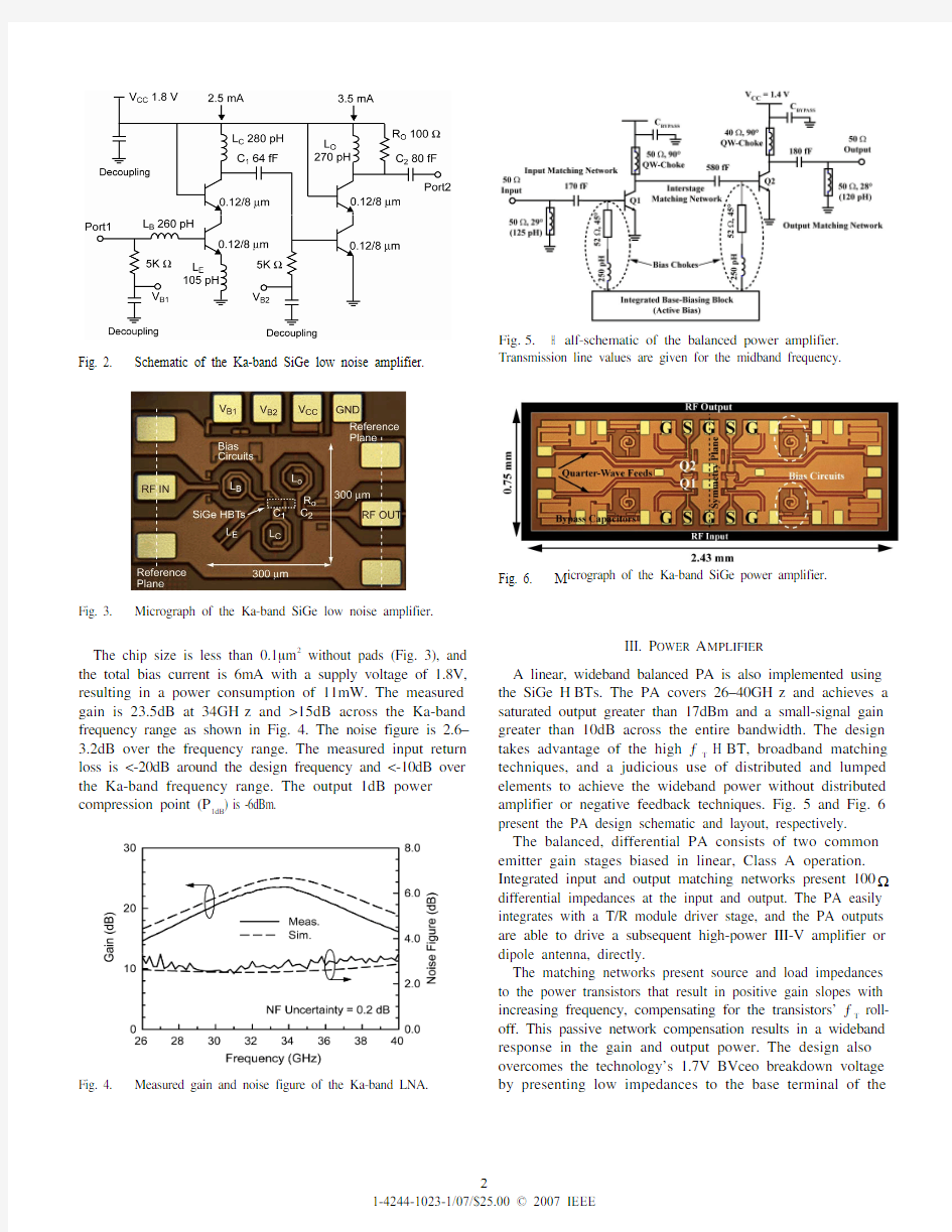
III. P OWER A MPLIFIER
A linear, wideband balanced PA is also implemented using the SiGe H BTs. The PA covers 26–40GH z and achieves a saturated output greater than 17dBm and a small-signal gain greater than 10d
B across the entire bandwidth. The design takes advantage of the high ?T H BT, broadband matching techniques, and a judicious use of distributed and lumped elements to achieve the wideband power without distributed amplifier or negative feedback techniques. Fig. 5 and Fig. 6 present the PA design schematic and layout, respectively.
The balanced, differential PA consists of two common emitter gain stages biased in linear, Class A operation. Integrated input and output matching networks present 100? differential impedances at the input and output. The PA easily integrates with a T/R module driver stage, and the PA outputs are able to drive a subsequent high-power III-V amplifier or dipole antenna, directly.
The matching networks present source and load impedances to the power transistors that result in positive gain slopes with increasing frequency, compensating for the transistors’ ?T roll-off. This passive network compensation results in a wideband response in the gain and output power. The design also overcomes the technology’s 1.7V BVceo breakdown voltage by presenting low impedances to the base terminal of the
Fig. 2. Schematic of the Ka-band SiGe low noise amplifier.
Fig. 3.
Micrograph of the Ka-band SiGe low noise amplifier.
Fig. 4.
Measured gain and noise figure of the Ka-band LNA.
Fig. 5. H alf-schematic of the balanced power amplifier. Transmission line values are given for the midband frequency.
Fig. 6.
M
icrograph of the Ka-band SiGe power amplifier.
power transistor at DC and the operating frequencies [3]. The resulting effective collector-emitter breakdown voltage allows the collectors’ output voltages to peak above 2.5V.
Fig. 7 presents the measured saturated and P 1dB output powers across frequency. The output saturated power (P sat ) is greater than 17dBm, and the output P 1dB is greater than 15.5dBm. Measured small-signal parameters are presented in Fig. 8. The gain is 13dB at midband, and the 3dB bandwidth extends from 25.5 to 41GHz (a fractional bandwidth of 47%).
The 1.83mm 2
PA consumes 525mW (375mA) from a 1.4V supply and achieves a peak PAE of 11.2%.
IV. P HASE S HIFTER
A 4-bit digital phase shifter with 22.5° phase resolution is designed using CMOS passive switches. The digital passive phase shifter has the advantage of simple control circuits and no power consumption from a digital-to-analog converter or the phase shifter itself. Using 4-bit phase shifters (having a maximum phase error of 11.25°), phased arrays can scan the
antenna beam almost continuously with a negligible decrease in array gain or increase in sidelobe levels.
The 4-bit phase shifter is implemented using 5 stages of phase-shifting elements (Fig. 9). Two 90° phase shifters are combined to form the 180° bit, and the 22.5°, 45°, and 90° bits are placed in series afterward. Each bit of the phase shifter can switch between a phase delay state (low-pass Π-network) and a bypass state [4]. The 45° bit is designed with two shunt capacitors (C p2). For the 22.5° bit, the parasitic junction capacitances (C jd , C js ) act as the shunt capacitors of the low-pass network. The chip area is less than 0.15μm 2, making it the smallest Ka-band phase shifter to-date.
Fig. 10 presents the measured absolute phase performance
Fig. 9.(a) Schematic and (b) micrograph of the Ka-band 4-bit
CMOS phase shifter.
(a)
(b)
Fig. 10. Measured insertion phase of the 4-bit phase shifter (16
different phase states).
Fig. 7. Measured saturated output power and power at the output-referred P 1dB .
Fig. 8. Measured small-signal parameters. The output-to-input isolation is >40dB across the operational band (not plotted).
of the phase shifter, and the RMS phase error is shown in Fig. 11. The phase error is less than 7.5° from 30–38GHz, which is much less than a 5th significant bit (11.25°). The input and output return loss of the phase shifter is less than -15dB over 30–38GHz and the insertion loss is -12±1.5dB at 35GHz.
V. SPDT S WITCHES
SPDT switches are also designed using CMOS transistors. At Ka-band frequencies, the primary limitation of CMOS switches is their source and drain junction capacitances. To improve the insertion loss of a series CMOS switch, the channel resistance of the CMOS transistor is usually reduced by enlarging the gate width. However, this increases junction capacitances and results in an increase of the on-state signal loss and a degradation of the off-state isolation. The effect of the junction capacitances can be reduced if the CMOS transistors are used as shunt switching elements.
Fig. 12 shows SPDT switches with shunt CMOS transistors. When the shunt switches are turned off, the series inductor L S forms a Π-network with the parasitic capacitances of the shunt transistors and also reduces input and output return loss. When the shunt switches are turned on, L O and C O resonate at 35GHz and present a high impedance (>200?) to the common input node. Fig. 13 shows the measured results of the CMOS SPDT
switches. The measured insertion loss is 2.5dB at 35GHz with a return loss less than -14dB. The measured isolation is higher than 25dB across the Ka-band frequency range. The input P 1dB of the SPDT switches is +13dBm.
VII. C ONCLUSION
The presented LNA, PA, phase shifter, and SPDT switches are designed for an integrated SiGe BiCMOS Ka-band phased-array T/R module. The LNA and PA are implemented using SiGe HBTs while the phase shifter and SPDT switches are based on CMOS switches. At 33–34GH z, the LNA achieves 23dB gain and 2.9dB noise figure, and the PA achieves 13dB gain and 19.4dBm output P sat with a peak PAE of 11.2%. The RMS phase error and gain error of the 4-bit phase shifter are less than 7.5° and 2.4dB, respectively, from 30–38GH z. The insertion loss and isolation of the SPDT switches are 2.5dB and >25dB, respectively.
A CKNOWLEDGEMENT
The authors thank Alfred Hung and Ed Viveiros at the U.S. Army Research Laboratories for their support.
R EFERENCES
[1] B.C. Kane, et al., “Smart Phased Array SoCs: A Novel
Application for Advanced SiGe HBT BiCMOS Technology,” IEEE Proceedings , pp. 1656-1668, Sep. 2005.
[2] S. P. Voinigescu, et al., “A scalable high-frequency noise model
for bipolar transistors with application to optimal transistor sizing for low-noise amplifier design,” IEEE Journal of Solid-State Circuits , vol. 32, pp. 1430–1439, Sep. 1997.
[3] M. Rickelt, H .-M. Rein, E. Rose, “Influence of Impact-Ionization-Induced Instabilities on the Maximum Usable Output Voltage of Si-Bipolar Transistors,” IEEE Trans. Electron Devices , pp. 774-783, April 2001. [4] R. Garver, “Broad-band diode phase shifter,” IEEE
Transactions on Microwave Theory and Techniques , vol. MTT-20, pp. 314–323, May 1975.
Fig. 12.
Schematic of the designed SPDT switches.
Fig. 13.Measured insertion loss and return loss of the SPDT switches. The measured isolation is >25dB over the Ka-band frequency range (not plotted).
Fig. 11. Measured insertion phase of the 4-bit phase shifter (16
different phase states).