BL6211中文资料

1.25 Watt Fully Differential Audio Power Amplifier
With Internal Feedback Resistors
Features
Fully differential amplifier
Improved PSRR at 217Hz(VDD>3.0V) 86dB (typ)
Power output at 5.0V & 1% THD 1.25W (typ)
Power output at 3.6V & 1% THD 0.6W (typ)
Ultra low shutdown current 0.01μA (typ)
Improved pop & click circuitry eliminates noises during turn-on and turn-off transitions
Thermal overload protection circuitry
No output coupling capacitors, bootstrap capacitors required
Unity-gain stable
External gain configuration capability
Available in space-saving package: 9-bump micro SMD and 8-pin MSOP8
General description
The BL6211 is a fully differential audio power amplifier designed for portable communication device applications. It is capable of delivering 1.25 watt of continuous average power to an 8? BTL load with less than 1% distortion (THD+N) from a 5V battery voltage. It operates from 2.2 to 5.5V.
Features like 86dB PSRR at 217Hz, improved RF-rectification immunity, the space-saving 8-pin MSOP8 and 9-bump micro SMD package, the advanced pop & click circuitry, a minimal count of external components and low-power shutdown mode make BL6211 ideal for wireless handsets.
The BL6211 is unity-gain stable, and the gain can be configured by external input resistors and internal feedback resistors.
Applications
Wireless handsets
Portable audio devices
PDAs, Handheld computers
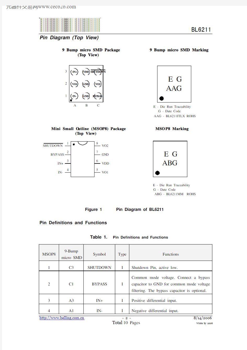
Pin Diagram (Top View)
E G AAG
E - Die Run Traceability G - Date Code
AAG - BL6211ITLX ROHS
9 Bump micro SMD Package
(T op View)
9 Bump micro SMD Marking
321
SHUTDOWN
B C
A GND IN-GND BYP ASS
VO2
VO1IN+VDD
1234
8765
SHUTDOWN
BYP ASS
IN+IN-VO2GND VDD VO1
E G ABG
E - Die Run Traceability G - Date Code
ABG - BL6211MM ROHS
Mini Small O utline (MSO P8) Package
(T op View)
MSO P8 Marking
Figure 1 Pin Diagram of BL6211
Pin Definitions and Functions
Table 1.
Pin Definitions and Functions
MSOP8 9-Bump micro SMD
Symbol Type Functions
1
C3
SHUTDOWN
I
Shutdown Pin, active low.
2 C1 BYPASS I Common mode voltage. Connect a bypass
capacitor to GND for common mode voltage filtering. The bypass capacitor is optional.
3 A3 IN+ I Positive differential input. 4
A1
IN-
I
Negative differential input.
MSOP8 9-Bump micro SMD
Symbol Type Functions
5 A2 VO1 O Positive differential output.
6 B3 VDD I Power supply
7 B1,B2 GND I Ground.
8
C2
VO2
O
Negative differential output.
Operation conditions and Electrical characteristics
Operation Conditions
Table 2.
Operation Conditions
Parameter Symbol Min Typ Max Unit Power Supply V oltage V DD 2.2 5.5 V Operating Temperature
Range
T A
-40
85
℃
ctrical Characteristics
Table 3.
V DD =5V (The following specifications apply for 8Ωload ,A V =1V/V ,T A =25℃,
unless otherwise specified.)
Parameter Symbol Conditions
Min Typ Max Unit VIN=0V , no load 2.5 5
Quiescent Power Supply Current I DD VIN=0V , R L =8Ω 4 8 mA
Shutdown Current I SD V SHUTDOWN =GND 0.01 1 μA Output Power P O THD=1%(max); f=1kHz 1.25 W Total Harmonic Distortion + Noise
THD+N
P O =0.6Wrms; f=1kHz
0.02
%
Vripple=200mV sine p-p
f=217Hz (note1)
-88 f=1kHz (note1) -83 f=217Hz (Note2) -83 Power Supply Rejection Ratio
PSRR F=1KHz (Note2)
-83
dB
Parameter Symbol Conditions Min Typ Max Unit
Common Mode
Rejection Ratio
CMRR f=217Hz V CM=200mV PP-78 dB Output Offset V OS VIN=0V 2 8 mV Shutdown V oltage
Input High
V SDIH 1.5 V
Shutdown V oltage
Input Low
V SDIL 0.5 V
Closed Loop Gain A V 36kΩ
Ri
40kΩ
Ri
44kΩ
Ri
V/V
Note1: Unterminated input Note2: 10Ωterminated input
Table 4.
V DD =3.6V (The following specifications apply for 8Ωload ,A V =1V/V ,T A =25℃,
unless otherwise specified.)
Parameter Symbol Conditions
Min Typ Max Unit VIN=0V , no load 2 4.5
Quiescent Power Supply Current I DD VIN=0V , R L =8Ω 3.5 7.5 mA
Shutdown Current I SD V SHUTDOWN =GND 0.01 1 μA Output Power P O THD=1%(max); f=1kHz 0.6 W Total Harmonic Distortion + Noise
THD+N
P O =0.4Wrms; f=1kHz
0.02
%
Vripple=200mV sine p-p
f=217Hz (note1)
-86 f=1kHz (note1) -83 f=217Hz (Note2) -83 Power Supply Rejection Ratio
PSRR F=1KHz (Note2)
-83 dB
Common Mode Rejection Ratio CMRR f=217Hz V CM =200mV PP -76 dB Output Offset V OS VIN=0V 2 8 mV Shutdown V oltage Input High V SDIH
1.5
V Shutdown V oltage Input Low V SDIL 0.5 V
Closed Loop Gain
Gain 36k ΩRi
40k ΩRi
44k ΩRi
V/V
Note1: Unterminated input Note2: 10Ωterminated input
Typical characteristics
2.2
2.0THD+N=10%
THD+N=1%
1.8
1.6
1.41.2
1.0800m 600m 400m
200m
0O u t p u t P o w e r (W )
Output Power vs Supply Voltage
R L =8Ω
Supply Voltage(V)
2.53
3.54
4.55
5.5
V DD =5V
f=1KHz THD+N ≤1%R L =8Ω
0.7
0.6
0.50.40.3
0.20.1
P o w e r D i s s p a t i o n (W )
Power Dissipation vs Output Power
Output Power(W)
00.20.40.60.8 1.0 1.2
V DD =3.6V f=1KHz THD+N ≤1%R L =8Ω
0.3
0.20.10P o w e r D i s s p a t i o n (W )
Power Dissipation vs Output Power
Output Power(W)
Ambient Temperature (℃)
20
40
60
80
100
120140160
Power Derating Curve
0P o w e r D i s s p a t i o n (W )
Micro SMD
MSOP
Frequency (Hz )
20
100
1K
10K 20K
10
10.1
0.001T H D +N (%)
0.01THD+N vs Frequency V DD =5V, R L =8Ω,P O =600mW
Frequency (Hz )
20
100
1K
10K 20K
10
1
0.1
0.001
T H D +N (%)
0.01
THD+N vs Frequency V DD =3.6V, R L =8Ω,P O =400mW
Frequency (Hz )
20
100
1K
10K 20K
10
1
0.1
0.001
T H D +N (%)
0.01
THD+N vs Frequency V DD =2.5V, R L =8Ω,P O =150mW
20kHz
1kHz
20Hz
THD+N vs Output Power
V DD =5V, R L =8Ω
10
1
0.1
0.001
T H D +N (%)
0.01
Output Power (W)
10m
100m 12
20kHz
1kHz
20Hz
THD+N vs Output Power V DD =3.6V, R L =8Ω
10
1
0.1
0.001
T H D +N (%)
0.01
Output Power (W)
10m
100m 1
20kHz
1kHz
20Hz
THD+N vs Output Power V DD =2.5V, R L =8Ω
10
1
0.1
0.001
T H D +N (%)
0.01
Output Power (W)
10m
100m 1
Frequency (Hz )
20
100
1K
10K 20K
-100
P S R R (d B )
PSRR vs Frequency
V DD =5.0V, R L =8Ω,input 10Ω Terminated
-90-80-70-60-50-40-30
-20-100C (BYPASS)=0μF
C (BYPASS)=1μF
C (BYPASS)=0.47μF
Frequency (Hz )
20
100
1K
10K 20K
-100
P S R R (d B )
PSRR vs Frequency
V DD =3.6V, R L =8Ω,input 10Ω Terminated
-90-80-70-60-50-40-30
-20-100C (BYPASS)=0μF
C (BYPASS)=1μF
C (BYPASS)=0.47μF
DC Common-Mode Voltage (V)
5
PSRR vs Common Mode voltage V DD =5.0V, R L =8Ω, 217Hz, 200mV PP
1
2
3
4
-100
P S R R (d B )
-90-80-70-60-50-40-30
-20-100
DC Common-Mode Voltage (V)
PSRR vs Common Mode voltage V DD =3.6V, R L =8Ω, 217Hz, 200mV PP
1
2
3
3.6
-100
P S R R (d B )
-90-80-70-60-50-40-30
-20-100
-200
-160-120-80-40040
80120
160200-200-160-120-80-40040
80120
160200Open Loop Frequency Response
Frequency (Hz )
Gain
Phase
G a i n (d B )
P h a s e (O )
-60
-50-40-30-20-100
1020
3040-180-140-100-60-202060
100
140180220
Closed Loop Frequency Response
Frequency (Hz )
Gain
Phase
G a i n (d B )
P h a s e (O )
Application
+
IN-
IN+
VO1
VO2
VDD
GND
Bias Circuitry
BYPASS
40k Ω
1μF
-C B 1μF R f C S 40k ΩR f
20k ΩR i
20k Ω
R i D i f f e r e n t i a l A u d i o I n p u t
8Ω
R L +-C B is optional SHUTDOWN
V IH
V IL
V DD /2
BL6211
Figure 2
Typical Differential Input Application
+
IN-
IN+
VO1
VO2
VDD
GND
Bias Circuitry
BYPASS
40k Ω
1μF
-C B 1μF R f C S 40k ΩR f
20k ΩR i
20k Ω
R i D i f f e r e n t i a l A u d i o I n p u t
8Ω
R L +-C B is optional
SHUTDOWN
V IH
V IL
V DD /2
BL6211
C i
0.39μF C i 0.39μF
+
IN-
IN+
VO1
VO2
VDD
GND
Bias Circuitry
BYPASS
40k Ω
1μF
-C B 1μF R f C S 40k ΩR f
20k ΩR i
20k Ω
R i Audio Input
8Ω
R L +-C B is optional
SHUTDOWN V IH
V IL
V DD /2
BL6211
C i
0.39μF C i 0.39μF
Figure4 Single-Ended Input Application