Ultra-Wideband Radar Sensors for Short-Range Vehicular Applications
Ultra-Wideband Radar Sensors for Short-Range
Vehicular Applications
Ian Gresham,Senior Member,IEEE,Alan Jenkins,Member,IEEE,Robert Egri,Member,IEEE, Channabasappa Eswarappa,Senior Member,IEEE,Noyan Kinayman,Member,IEEE,Nitin Jain,Member,IEEE, Richard Anderson,Frank Kolak,Ratana Wohlert,Shawn P.Bawell,Member,IEEE,Jacqueline Bennett,Member,IEEE,
and Jean-Pierre Lanteri,Member,IEEE
Invited Paper
Abstract—The recent approval granted by the Federal Com-munications Commission(FCC)for the use of ultra-wideband signals for vehicular radar applications has provided a gateway for the introduction of these sensors in the commercial arena as early as2004.However,the rules governing the allowable spectral occupancy create significant constraints on the sensors’opera-tion.This is further complicated by the variety of applications that these sensors are being required to fulfill.A review of the motivation for the development of these sensors is followed by a discussion of the consequent implications for waveform design and limitations on system architecture.Other practical considerations such as available semiconductor technology,packaging,and assembly techniques are reviewed,and results are presented for conventional surface-mount plastic packages illustrating their usefulness in the greater than20-GHz frequency range.Suitable antenna technology for wide-band transmission is presented that is compliant with the specific restrictions stipulated in the FCC ruling.Finally,all of these considerations are combined with the presentation of a compatible integrated-circuit-based transceiver architecture.Measured results are presented for several critical circuit components including a+12-dBm driver amplifier for the transmitter,an RF pulse generator that can produce sub-1-ns pulses at a carrier frequency of24GHz,and a single-chip homo-dyne in—phase/quadrature down-conversion receiver that has a cascaded noise figure of less than7dB.All circuit components are fabricated in SiGe.
Index Terms—Automotive,radar,SiGe,ultra-wideband(UWB).
I.I NTRODUCTION
A FTER YEARS of public hearings and rule-making de-
bates,the approval granted by the Federal Communica-tions Commission(FCC)through its modified and amended 47CFR Part15regulations allocates over7GHz of usable un-licensed spectrum between3.1–10.6GHz for communications and imaging systems based on ultra-wideband(UWB)devices [1].This ruling has been the subject of much interest and,in-deed,controversy[2]–[6].A large number of both proponents
Manuscript received August4,2003;revised May13,2004.
I.Gresham,A.Jenkins,R.Egri,C.Eswarappa,N.Kinayman,R.Anderson, R.Wohlert,S.P.Bawell,J.Bennett,and https://www.wendangku.net/doc/3f19058144.html,nteri are with Corporate Research and Development,M/A-COM,Lowell,MA01853USA.
N.Jain is with Anokiwave Inc.,San Diego,CA92130USA.
F.Kolak is with the Mitre Corporation,Bedford,MA01730USA.
Digital Object Identifier10.1109/TMTT.2004.834185and opponents of the change in the regulations have been unable to agree upon the level of maximum radiated emission levels that unlicensed users of the spectrum must adhere to in order that existing radio,communication,and other licensed services will be unaffected by harmful interference caused by UWB de-vices.However,the potential ability for UWB devices to occupy spectrum concurrently with existing systems,thereby allowing the scarce spectrum to be used more efficiently,has led to the approval being granted[1].The National Telecommunications and Information Administration(NTIA),who are responsible for the licensing and control of federal and government fre-quency bands in the U.S.,were particularly concerned with the potential cumulative effect sensors could have on the global po-sitioning system(GPS)bands,with the consequence that UWB devices are required to have very low spectral emissions in the 960–1610-MHz band[7].
In addition,although maybe less well appreciated,the ruling also approved a second allocation of an unlicensed7-GHz wide spectrum between22–29GHz that is intended exclusively for vehicular radar systems.These systems are intended to detect the location and movement of objects near a vehicle by devel-oping a continuously updated360-radar map of the vehicles’surroundings.Depending upon the sophistication of the system and its intended purpose,this would enable features that can provide,amongst other functions,collision avoidance,enhanced airbag activation,and improved road handling through interac-tion with other vehicular dynamic systems.This allocation is no less controversial than the lower frequency ruling due to its requirement for coexistence with various radio astronomy and other sensitive frequency bands.In fact,it may be more prob-lematic in that it is not just adjacent to these bands,but indeed overlaps them.As we shall see,this has had a profound influ-ence on system and waveform design,and on the perceived way that systems will be introduced,first in the U.S.,and eventually in the global marketplace.
In order to understand the rationale for such a controversial move,it is worthwhile reviewing the motivation for the intro-duction of automotive radar systems.In Section II,an overview of the requirements for and of short-range radar(SRR)sensors is used as an introduction to the details of the FCC UWB ruling for vehicular radar applications.Section III considers this ruling
0018-9480/04$20.00?2004IEEE
in the context of its implications for waveform and system de-sign,and discusses some of the tradeoffs that were considered in architecture selection.Details of sensor level operational performance and consequent system level performance are shown.Section IV highlights the technological choices—me-chanical form,semiconductors,packaging,interconnects,and interfaces—that are imposed by the architecture selection,but more importantly,by both the constraints of the marketplace and the need for the sensors to be networked with other func-tions on the vehicle.In Section V,a specific implementation of a generic integrated-circuit(IC)-based SRR is shown as an example[8]–[10]along with several examples of measured circuit-level performance to demonstrate compliance with the sensor level requirements detailed in Section III.Finally,some comments on the future of UWB radar are presented.
A.Case for Vehicular SRR
The subject of automotive radar is not new,and developments have been occurring on a regular basis,as reported in the tech-nical literature for many years[11].One of the main barriers to widespread introduction to date has been the ability to fulfill the extremely demanding technical requirements at a cost level that the average consumer will find palatable.However,signif-icant advancements have been made due to the strong support that the introduction of such sensors has from the automotive industry in general[12].They perceive that the increased safety such vehicles offer to the consumer will provide a differentiating competitive advantage.A far more important,and indeed more persuasive,argument for the introduction of smart vehicles is that any increase in safety in automobiles should have a conse-quent effect in reducing the number of fatalities that occur every year.It is,of course,this second argument that has found favor with the various governmental and regulatory agencies around the world that are required to pass the corresponding legislation. Consider,in2002,the number of occupant fatalities in road crashes in the U.S.increased for the first time since1990to an estimated figure of over42000people annually.The total number of fatalities per year in the U.S.has been relatively con-stant at around40000since1991[13],despite improvements in vehicle safety design and features.This unacceptably high level led to two major initiatives in the U.S.for the Department of Transportation to work in partnership with industry to develop and deploy effective collision avoidance products[14],[15]. In2001,the National Transportation Safety Board(NTSB) concluded that the benefits and effectiveness of collision warning systems(CWSs)and adaptive cruise control(ACC) [16]were of public importance.Independent of this,a similarly high level of fatalities in the European Union—over44000in 1998—led to the European Commission(EC)setting a goal of a50%reduction in the number of annual road deaths by2010 [17],[18].Although this ambitious target can probably not be reached through the introduction of new technology alone,the EC concluded that one of the vital steps in reaching this goal was through the introduction and implementation of Advanced Driver Assistance Systems,and that a key component of such systems was the introduction of UWB radar at24GHz[18].In September2003,the EC committed to work with the European Conference of Postal and Telecommunication
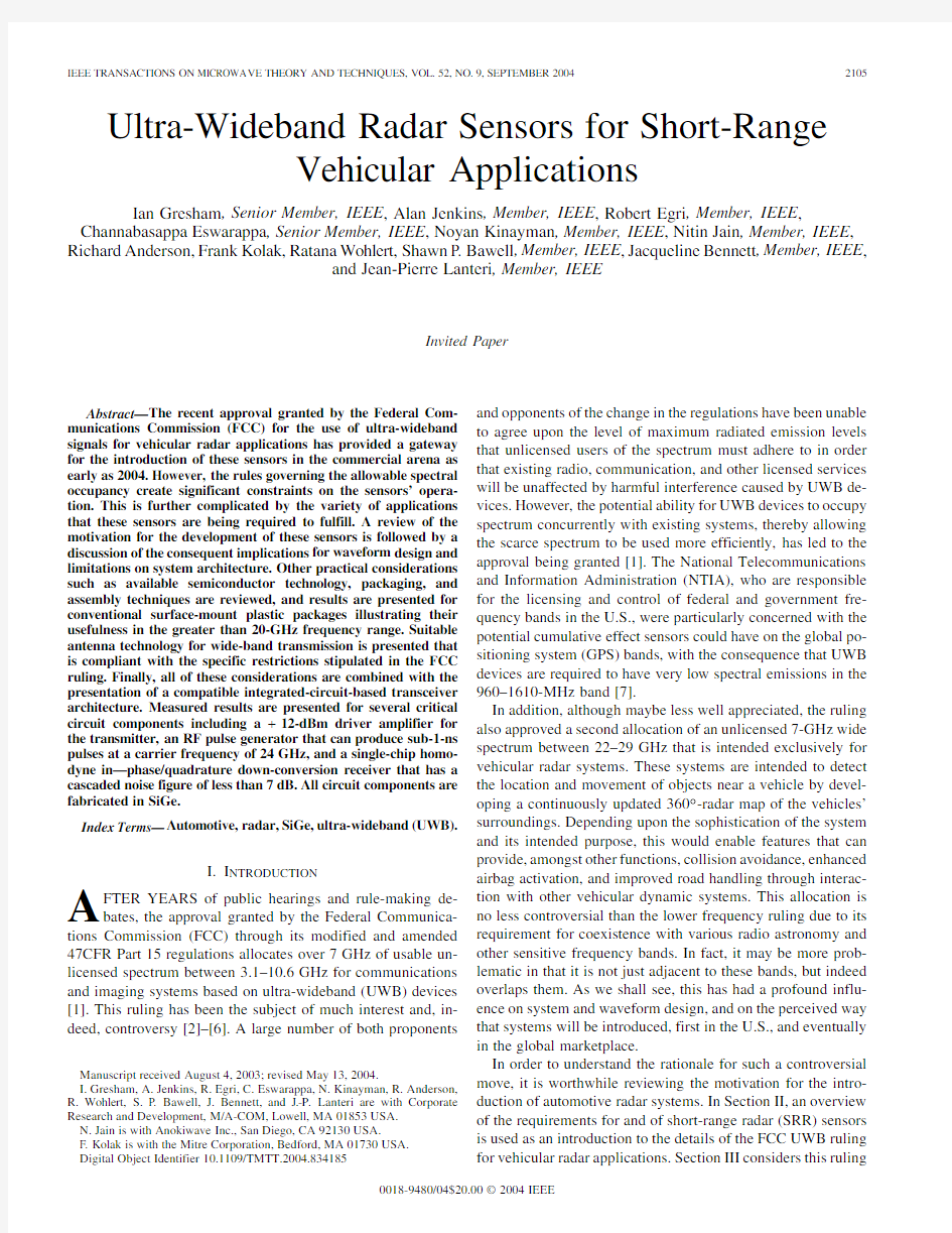
Administrations Fig.1.Collision probability as a function of increased driver reaction time for varying crash scenarios[22].
(CEPT)to remove the regulatory barriers that prevented the adoption of UWB radar in Europe to facilitate the rapid deployment of SRRs at24GHz with an eventual migration to 79GHz[19].
https://www.wendangku.net/doc/3f19058144.html,plete Environment Sensing for Automotive Vehicles Given the multiplicity of various driving and traffic sce-narios,a variety of active(that provide automatic intervention) and passive(that provide driver information)safety systems are required to give a vehicle the capability to not only perceive and understand its environment,but to also act upon it.The more important of these systems in terms of traffic and object aware-ness are largely vision—both video and infrared(IR)—and radar based[20],[21].This emphasis on introducing a variety of sensing technologies to provide a vehicle with a complete environmental awareness as a means of improving safety arises from some interesting statistics.It has been estimated that95% of all road accidents involve some human error and that,in76% of all accidents,a human is solely to blame.Associated with this is the thought-provoking statistic that almost all collisions at intersections,with oncoming traffic,and rear-end impacts, could be avoided if driver reaction time was shifted forward by2s[22],[23],as presented in Fig.1.Confirmation for this comes from a related subject of much research whereby event data recorders(i.e.,black boxes)are added to vehicles to monitor,record,display,or transmit(Tx)pre-crash,crash,and post-crash data element parameters from a vehicle[24].It is postulated that almost all of these accidents could be avoided through the introduction of CWSs and automatic vehicle interventions[18],[25]through the use of a hybrid sensor array to form a safety belt around the vehicle.
A typical schematic of one of these sensor arrays is shown in Fig.2.Radar is perceived as a key element in the sensor array due to its ability to offer an immunity to weather condi-tions that is unavailable with other technological solutions.It also offers the vehicle manufacturers a stylistic advantage over ultrasonic or video sensors in that it can be mounted behind a
GRESHAM et al.:UWB RADAR SENSORS FOR SHORT-RANGE VEHICULAR APPLICATIONS
2107
https://www.wendangku.net/doc/3f19058144.html,plete environment sensing for automobiles is achieved through a hybrid array of multiple sensor technologies and functions.The functions and typical system range of operation shown are representative only.Short-range sensing requirements for the radar sensors are envisaged to cover a variety of applications,each with differing needs for range,update rate,range resolution,and other key system parameters.
fascia that (although dissipative)can be considered transparent to the radar signal without requiring specific cutouts or sim-ilar accommodations.The longer-range ACC systems have been readily available in production vehicles for over three years,and are being increasingly supplemented by video systems to im-prove the quality of information available.In the ACC systems,a narrow beam (2or 3)is typically scanned over the front of the vehicle over an azimuth variation
of 5
to 8,and the information used to regulate its speed so that a sufficient safety margin of distance to the vehicle ahead is maintained.These systems have a necessarily narrow scanning angle (for adequate azimuth resolution of objects that may be 150m ahead),and a range resolution of 1–2m.This distance requirement also means that the high-gain antennas have a necessarily small beamwidth that inhibits their usefulness in their ability to detect and track objects at close range
(20m).Increasing the number of beams to increase the scanning angle is problematic for two reasons.Firstly,the antenna has to become more complex and,therefore,more expensive.Secondly,as the number of beams is increased,the scan rate (and,hence,dwell-time per range gate)is affected.The update rate for tracking algorithms is particularly impor-tant for very short-range operation.A further consideration is the desire to have 360coverage around the car.A single sensor is clearly not a suitable solution,and a system comprised of mul-tiple networked sensors that are distributed at appropriate loca-tions is required [26].The precise number of sensors is a func-tion of the amount of coverage required,and the corresponding coverage overlap of adjacent sensors.However,depending upon the azimuth coverage of each sensor,anywhere from 4to 16in-dividual radar sensors may be required,with placement biased
toward the front bumper,followed by the rear bumper corre-sponding to the statistically highest crash areas.Proportionally fewer sensors are required for sideways looking operation.C.Short-Range Sensors—The Requirement for UWB Radar at 24GHz
Fig.2illustrates the variety of applications that the short-range sensors are required to fulfill [27],[28].They range from simple parking aid functions to more elaborate pre-crash detec-tion,and stop-and-go or short-range cruise control functionality.The precise requirements for these applications differ between each other,and also between individual vehicle manufacturers.However,it is possible to define some typical specifications,at least for the more commonplace applications.A summary of some of the key requirements for four differing sensing func-tions is given in Table I.These represent the more immediate of the applications that automotive manufacturers want to in-troduce on vehicle platforms as a first step to the eventual in-tegrated sensor solution.Parking aids are already available on many vehicles through the use of ultrasonic sensors.However,radar sensors offer potentially superior range performance,as well as being less susceptible to inclement weather conditions,or requiring custom cutouts in the bumper fascia.The pres-ence of the radar sensor is also considered to then be a gateway to some of the more complex applications,as it can be more easily integrated into the entire sensor network and its opera-tion extended,for example,from being a simple parking aid to a blind-spot detector.One of the more demanding applications is the extension of ACC to a short-range stop-and-go function-ality.This requires not only good range resolution,but also the
2108IEEE TRANSACTIONS ON MICROW A VE THEORY AND TECHNIQUES,VOL.52,NO.9,SEPTEMBER 2004
TABLE I
S UMMARY OF T YPICAL S HORT -R ANGE S ENSOR S YSTEM R EQUIREMENTS FOR
A V ARIETY OF D IFFERING A
PPLICATIONS
ability to detect and track objects such as a bicycle at ranges of over 20m initially,leading to perhaps 30–40m over time as systems become more complex and mutually dependent.The longer-range ACC systems have particular difficulty in moni-toring the corners of vehicles,for example,and are looking to the short-range sensors to provide an increased warning or re-action time for cut-in https://www.wendangku.net/doc/3f19058144.html,stly,pre-crash detection net-works are seen as being essential,but demanding,applications that are critical to improving safety.An example of such a func-tion is pre-impact sensing,whereby the closing velocity of an object that is projected to impact a vehicle may be tracked in order that the threshold voltage for airbag deployment may be dynamically adjusted.This is especially important in side-im-pact situations where extra milliseconds for airbag firing could be important.Despite the differing requirements for these appli-cations,the concept of a networked sensor system,plus the cost requirements,oblige a common sensor architecture and design that is adaptable to be used in each https://www.wendangku.net/doc/3f19058144.html,worked Sensor Operation
A distributed networked sensor structure for the radar re-sults in a system that has a hierarchical detection and tracking process.The totality of information available for compiling and updating the radar map is comprised of information from each of the discrete sensors,plus additional data from the other sen-sors that are included in the hybrid sensor network.The infor-mation available from a single sensor is,therefore,a subset of the total information required by the total radar system.Each sensor consists of an RF/IF front-end that forms the air inter-face —Tx and receive (Rx)circuitry and antennas —plus associ-ated control and signal circuits.Local digital signal processing (DSP)in each sensor is required to perform first tier detection analysis by generating a priority list of detected objects within the sensors ’field of view.The objects and their associated pa-
rameters —range,amplitude,and relative-velocity —are sent via a network to a central processor or radar decision unit (RDU).The RDU is also networked via the controller area network (CAN)-bus to accept inputs from other systems within the ve-hicle,as shown in Fig.3.The entirety of the separate sensor in-puts are then analyzed by the RDU,which performs higher level detection and tracking algorithms,and initiates appropriate de-cisions and instructions that are output to the network bus.The requirements for detection ability for each sensor are,therefore,different for the complete radar system.For example,typical
numbers for the probability of
detection
and probability of false
alarm of an object may be 0.9
and
10,respec-tively,at the individual sensor level,but are substantially im-proved at the system level.Here,we will focus on the issues of the discrete UWB SRR sensor that forms a component part of the complete networked radar.For a comprehensive discourse on the much more complex issue of how the networked system functions,see Klotz [26].
II.UWB S ENSORS AND THE FCC P ART 15R ULING The key specification common to all of the differing appli-cations that the 24-GHz sensor is required to fulfill is that of range resolution,as indicated in Table I.The accuracy of time information and,therefore,the ability to precisely determine an object ’s location,is inversely proportional to the signal band-width.The precise measurement of object movements is essen-tial for the prediction of trajectories and the prevention of false alarms.For a requirement of sub-10-cm resolution,therefore,the spectral occupancy of the main lobe of the incident wave has to be at least 3-GHz wide and more likely needs to be of the order of 4-GHz wide to allow for errors,variations,and de-sign margin.The availability of such a broad spectral frequency band has to be balanced with other practical considerations.The gain,or focusing ability,of an antenna is proportional to the antenna aperture.The antenna of each sensor,therefore,has to be small enough that an aperture of suitable electrical size can be physically mounted in the restrictive space behind a vehi-cles ’bumper fascia.In addition,as a percentile of center fre-quency,it becomes easier to produce antennas that support sig-nals of at least 4-GHz wide by increasing the frequency of op-eration.However,there are also several practical considerations that conversely argue for as low an operating frequency as pos-sible [29].The requirement for multiple sensors in a networked configuration forces the average cost per sensor to be low.De-spite the advances made in ACC radar at 77GHz,technology has not yet progressed enough such that a 77-GHz multisensor system can be cost competitive.In addition,fascia and atmo-spheric loss is far higher at 77GHz than at 24GHz —an impor-tant issue in any power-limited https://www.wendangku.net/doc/3f19058144.html,stly,it is believed by Short-range Automotive Radar frequency Allocation (SARA)1that the short-range sensor market is more likely to grow with a frequency allocation that is not dependent upon rapid technolog-ical advances.Weighing all of these factors together,the (nearly)
1SARA
is a consortium of automotive manufacturers and suppliers that was
formed in Spring 2001to coordinate frequency allocation issues for SRR sensors with the FCC,European Telecommunications Standards Institute (ETSI),and the International Telecommunication Union (ITU).
GRESHAM et al.:UWB RADAR SENSORS FOR SHORT-RANGE VEHICULAR APPLICATIONS
2109
Fig.3.Schematic representation of multiple short-range sensors connected to a local network.Each sensor passes a detected object list onto the network for analysis in the RDU.
global industrial,scientific,and medical (ISM)frequency allo-cation around 24.125GHz is ideal.
Well,almost.Unfortunately,there are several licensed frequency bands that surround the 24.125-GHz ISM band that are used for predominantly low-power and sensitive appli-cations.In particular,a global spectrum allocation between 23.6–24GHz is used for radio astronomy and remote sensing.It is this band,in particular,that has caused consternation amongst other spectrum users,particularly the European Space Agency (ESA),European Meteorological Satellite Service (EUMETSAT),Committee on Radio Astronomy Frequencies (CRAF),and others [30].Passive satellite-based sensors are used by the Earth Exploration Satellite Service (EESS)for monitoring water vapor and trace gas concentration in the Earth ’s atmosphere,and the lifting of the background noise level through the introduction of millions of albeit,low-level,radiators is seen as a cause for concern.There are also concerns about the effect of increases in wide-band spectral emissions on fixed service communications (also in the 23–26-GHz band in Europe).This has led to the specific regulations imposed by the FCC,which calls for reduced emissions at certain elevation angles above the horizon over time.The specification is written in terms of an emitted power spectral density,or effective isotropic radiated power (EIRP),which allows for either a reduction in the peak transmitted power or,as is more likely,a reduction in the elevation sidelobes of the Tx antenna.Similar proposals in Europe are at the time of writing still under consideration by the ETSI.One mitigating solution that is the subject of much research —notably by the Radarnet
consortium 2—is the proposal by SARA in conjunction with the European Radiocommunications Office (ERO)to impose a sunset date on the introduction of 24-GHz radar systems of 2014or ten years after their introduction,whichever is later.In conjunction,SRR sensors would slowly migrate in frequency to be based at 79GHz.This would set an upper limit on the maximum number of sensors produced at 24GHz and,thus,limit the increase in background noise that the EESS sensors would be exposed to.It should be noted that the corresponding spectrum at 79GHz has also yet to be allocated.
Table II summarizes the key elements of the Part 153ruling governing UWB radars for vehicular applications.The asso-ciated spectral mask is illustrated in Fig.4.To be considered an UWB device,the fractional bandwidth of the spectrum measured at the 10-dB point from the peak must be at least 20%or 500MHz,regardless of the fractional bandwidth.The vehicular radars must operate between 22–29GHz in such a way that the center frequency and the frequency at which the highest level emission occurs must be greater than 24.075GHz.Thus,to be considered UWB,the vehicular radar must have at least 500-MHz bandwidth to satisfy the regulations.Normally,the spectral density of the average emission in this band should not exceed 41.3dBm/MHz.To reduce potential interference
2Radarnet —A
European-based consortium of car manufacturers,electronics
suppliers,and researchers who are developing SRR applications for 77GHz.[Online].Available:https://www.wendangku.net/doc/3f19058144.html,.
3The Electronic Communications Committee,CEPT issued an approval no-tice for the allocation of the 77–81-GHz spectrum for Automotive Short-Range Radars on March 19,2004.
2110IEEE TRANSACTIONS ON MICROW A VE THEORY AND TECHNIQUES,VOL.52,NO.9,SEPTEMBER 2004
TABLE II
S UMMARY OF THE K EY E LEMENTS OF THE FCC R ULING G OVERNING
UWB R ADARS FOR V EHICULAR A PPLICATIONS
[1]Fig.4.Spectral mask of the UWB ruling for vehicular radar.Note that the peak radiated emission limit overlaps the 23.6–24-GHz astronomical band and,thus,has specific additional limitations imposed in this area.
with radio astronomy observations and passive earth sensing satellites,the FCC further limits the radiated emissions by requiring that,in the 23.6–24.0-GHz band,the EIRP of the antenna sidelobes beyond 30above the horizontal plane not exceed 66.3dBm/MHz until 2010,and dropping to 76.3dBm/MHz beyond 2014.In addition to the average limit of 41.3dBm/MHz,the FCC also effectively limits the peak EIRP density emission to 17dBm/MHz in a 50-MHz band around the frequency of the highest power emission.These two constraints effectively dictate a maximum duty cycle for a sensor in pulsed operation to around 0.4%to take full advantage of the average power specifications.The FCC is clearly con-cerned about the interference generated by potentially millions of radars operating simultaneously.Of course,there are also limits placed on spurious emissions;see the details in [1].One proposed solution to the restriction on elevation sidelobes is to center the spectrum of the transmitted signal above 25GHz so
that the first null of
the
spectrum falls at the restricted band,thus reducing some of the demands upon antenna design.This may well become the preferred interim solution,although early sensor production is still planned for an ISM-band center frequency.
TABLE III
S UMMARY OF THE P RINCIPAL S HORT -R ANGE S ENSOR L EVEL R EQUIREMENTS
FOR O BJECT D
ETECTION
III.S YSTEM A RCHITECTURE AND W A VEFORM D ESIGN Table III summarizes some of the more important operational and practical requirements for a generic short-range sensor.By combining an understanding of the EIRP spectral limitations with our knowledge of the operational performance require-ments of the networked radar system,it becomes possible to compare the relative merits of different sensor architectures,and select the most appropriate.
A.Sensor Architecture Considerations
One can broadly characterize radar architectures of interest in vehicular applications into three generic types,which are:1)pseudorandom noise (PN)coded continuous-wave (CW)radars;2)classical frequency-chirped systems;and 3)pulsed radars [31].Simple CW Doppler radar systems are not consid-ered here,as almost all of the vehicular applications require the detection of zero relative velocity https://www.wendangku.net/doc/3f19058144.html,mon to all of these techniques is the ability to employ a process known as pulse compression.This is a traditional technique for enhancing radar performance and may be used to improve sensitivity for detecting targets at long range.It is also possible to combine techniques to form hybrid radar systems.
Frequency chirp radars that use pulse compression are ideal for long-range higher power applications.Resolution is related to how fast and over how wide a bandwidth it is possible to generate a well-defined chirp.Close-range and closely spaced targets also put stringent requirements on local oscillator (LO)phase noise.Both of these requirements can be challenging in the UWB context in any cost-effective manner.
PN-coded radar —essentially a spread-spectrum-type system —also provides the possibility for pulse compression,often referred to as coding or processing gain in the context of PN codes.Here,flexibility exists with the choice of the code,allowing designers to trade various performance parameters,with the limitation that dynamic range is often restricted by code auto-correlation properties [28].The ability to assign different codes to systems that share the same spectrum also provides an inherent resilience to interferers making it a good
GRESHAM et al.:UWB RADAR SENSORS FOR SHORT-RANGE VEHICULAR APPLICATIONS2111
choice for a multiradar unit system such as that envisaged for vehicular use.However,to maintain the high range resolution, a very fast set of code generators is required,with typical implementations requiring each code generator to be run at a well-defined frequency with a constant offset between one another.This would require two phased-locked loops,which could add significant cost.However,the principal disadvantage of PN-coded radars is that of dynamic range.In addition to the significant variation in the target-return signal level that occurs through the ratio of minimum to maximum range must be added the diversity of radar cross sections(RCSs)that complex targets may present to the radar system.It is extremely difficult to maintain adequate isolation between the Tx and Rx antennas such that the required dynamic range may be achieved,bearing in mind that there is a wide variation(and little influence that may be had)in the mounting environment of the sensor behind the vehicles fascia.This often restricts the operating range of the PN-coded radar to distances of less than10m.
Longer-range detection requirements force a classical pulsed radar solution to be considered.Although complex timing and delay circuitry is required,isolation between the Tx and Rx can be increased somewhat due to its time-gated nature,hence,en-hancing the dynamic range.Other desirable attributes include good range accuracy,clutter reduction,and multipath resolu-tion[31].Pulsed radar is also perhaps one of the simplest archi-tectures to implement,thus potentially making it the most cost effective.However,again the requirement of a radiated spec-trum of at least3-GHz wide proves challenging.The minimum time delay between two consecutive pulses is determined by the closest range gate.A two-way flight time of1ns(corresponding to a target at a range of0.15m)implies that either two sources are used(to generate the first IF frequency for a heterodyne re-ceiver)or a single source has to slew over at least3GHz and be stable in less than1ns.Neither is practical,which directs us toward a homodyne receiver architecture with direct conversion to baseband.The peak-power limitation of the FCC ruling also limits the amount of radiated energy that may be transmitted. This can result in short-pulse radars being limited in range.Even though the sensors are only required to detect objects at up to 20-m and eventually30-m distances,it is necessary to employ techniques such as a random pulse repetition interval jitter,in-creased dwell times for selective range gates,and pulse-com-pression techniques to maximize the amount of energy trans-mitted within the available spectrum https://www.wendangku.net/doc/3f19058144.html,stly,as a result of the zero IF structure,there is the added problem of detecting the signal in the presence of often large dc offsets.However,the in-herently high isolation between range bins that can be achieved relatively easily using switches makes this the most cost-effec-tive solution given the other challenges.
B.Time-Gated Correlation Receiver Architecture
The correlation receiver is a time-domain equivalent of the optimal frequency-domain matched filter receiver[32].Corre-lation occurs by multiplying the incident signal from the Rx an-tenna with a locally generated replica of the transmitted pulse, and integrating the result.A simplified schematic diagram of a second-generation pulsed-SRR sensor is shown in Fig.5.The RF front end is separated into three distinct sections,which are:1)Tx circuitry;2)Rx circuitry;and3)control and processing circuits.The operation of the sensor is as follows.A pulse of RF energy is transmitted from the sensor at a
time,as deter-mined by a trigger signal.This event simultaneously activates a local delay generator that commences to wait for a certain time until a second trigger is activated,which is the indication for the receiver to sample its output and store the sampled signal for further processing.Before the second trigger is activated,the Tx/Rx select switch is toggled between the Tx antenna and the LO ports of the receiver.The broad-band input signal from the Rx antenna is then multiplied with a locally generated replica of the Tx signal,resulting in pulse expansion if the two signals are time correlated.The result of the multiplication operation is in-tegrated in the baseband filter.In the pulse radar,this is done on a pulse-by-pulse basis,with the consequence that,under ideal conditions,the receiver output would be zero if the pulses do not overlap in the time domain,and a maximum that is propor-tional to the magnitude of the received pulse if they are coin-cident.As there is a direct relationship between the duration of the pulse and its spatial resolution,this coincidence in time fixes the range resolution.Thus,by varying the time delay between these two trigger events,it is possible to determine the presence of multiple objects at varying distances from the sensor corre-sponding to the minimum time delay(closest in range)to the maximum time delay(farthest in range).Of course,in reality,we have real-world issues to contend with such as wide-band noise, the presence of interferers,clutter(multiple unwanted reflec-tions),dynamic range limitations,pulse smearing,and all of the traditional issues that make receiver design challenging.Mul-tiple samples of the receiver output are necessary,therefore,to average the returned signals corresponding to a particular time delay(or range gate)and determine the fundamental question of any radar system:was an object detected or not?The prob-ability of making this decision correctly is proportional to the number of pulses collected in the receiver for each range gate. This is,in turn,a function of the gate length,which is deter-mined by the required range resolution,and update rate of the radar map.Detection algorithms that can dynamically vary the amount of dwell time per range gate and,thus,spend a propor-tionally longer time collecting signal returns from those farthest from the sensor are,therefore,beneficial.For example,a rider on a motorbike may present an RCS of only several square me-ters,as compared with a typical automobile,which may be an order of magnitude higher[33].In order to reliably detect a mo-torbike at a range of greater than20m,it may be necessary to collect and average the returns from a few hundred Tx pulses. The signal-to-noise ratio for a single pulse may be negative,and only by averaging noise over a period of time does it becomes possible to make a detection decision.
C.Interference Issues and Mitigation
A large variation in the magnitude of the returned radar signal is not the only challenge that the sensor has to contend with. There are at least three classes of interference relevant to the UW
B vehicular radar.These are:1)the spurious emissions gen-erated by the sensor and radiated as radio frequency interference (RFI);2)spurious emissions radiated in-band as a consequence of finite switch isolation;and3)in-band interferers or jammers
2112IEEE TRANSACTIONS ON MICROW A VE THEORY AND TECHNIQUES,VOL.52,NO.9,SEPTEMBER
2004
Fig.5.Simplified schematic diagram of the SRR RF front-end.An object at range R is detected by measuring the elapsed time between a transmitted pulse and a correlated received signal.The transceiver is split into three distinct functions.
that originate from other sensor systems.The first and only class important to regulatory agencies is the spurious emissions the radar generates.These emissions,of course,must be appropri-ately filtered in accordance with regulatory spectral emission limits.In addition,there is also a spurious emission from the pulse radar that is caused by the finite switch isolation.This is illustrated in Fig.6.Since the oscillator is continuously running,finite switch isolation results in a CW tone being continually transmitted.Although the switches used to generate the short Tx-pulse reduce the amplitude of this tone to a level that satisfies the FCC requirement on CW leakage,the signal can still cause a significant problem.The signal is reflected from the target under observation and interferes with the receiver ’s detection process by reducing its effective radar cross-sectional dynamic range;it also increases the false alarm rate and/or reduces detection probability.Similarly,the last important class of interferers to the UWB radar receiver is jamming arising from CW signals that appear in the receiving band —e.g.,from other UWB
radars
Fig.6.Measured output spectrum of the pulse former being driven to produce a 1-ns pulse with a PRF of 30MHz.The 24.15-GHz LO CW leakage can be clearly seen.
employing FM-CW-type architectures.A particularly difficult scenario is if another vehicular radar is facing the SRR only a
GRESHAM et al.:UWB RADAR SENSORS FOR SHORT-RANGE VEHICULAR APPLICATIONS 2113
few meters away.This jamming can potentially saturate the re-ceiver unless the latter is carefully designed.These interferences can be mitigated to some extent in a coherent radar by changing the carrier frequency from pulse to pulse.The radar is also sus-ceptible to other UWB pulse radars,and it can jam its own sisters mounted on the same bumper,although the time-gated opera-tion helps to an extent,as does randomizing,or staggering,the pulse epochs.A further benefit of this randomized pulsing is in meeting the spectral emission limits of the FCC by spreading the radiated energy more evenly across the operating bandwidth.
IV .S UITABLE T ECHNOLOGY FOR UWB S ENSORS
AND I NTEGRATED S ENSOR D ESIGN
Currently,sensors scheduled for production are fabricated using conventional surface-mount components and distributed transmission-line-based circuits with discrete baseband pro-cessing and control circuitry.Aside from cost,repeatability,and yield issues in following this approach,the wide instanta-neous bandwidth of sub-1-nS-long pulses makes the design of distributed circuits problematic.It is also difficult to increase or vary the functionality without increasing cost.Fig.7shows a photograph of these first-generation sensors and an exploded view of their construction.It should be noted that Fig.7does not represent an implementation of the sensor depicted in Fig.5.The historical path in the electronics industry for reducing cost,and improving and increasing functionality,has been to migrate toward IC-based solutions.Fig.5represents an evolution of the first-generation UWB sensor due to be launched in production in 2005[8].The baseband and microwave circuitry are realized using three separate ICs —a single-chip Tx IC,a single-chip Rx IC,and an application-specific integrated circuit (ASIC)that produces control signals and performs pre-processing of received data for formatting and interfacing with the vehi-cles ’CAN-bus.Separation of the Tx and Rx functions into separate ICs is a pragmatic decision based upon the operating environment.The large dynamic range required of the sensor has receiver sensitivity as one of its principal limitations.By mounting the noise sensitive LNA and receiver in a different location than the signal source and potentially noisy control signals gives the designer the most control over isolation between the two functions.The following sections provide an overview of the operation of the transceiver,followed by a brief review of the practical implications for realizing the critical circuit functions in an IC.A.Tx IC Operation
The Tx IC for the UWB sensor has a CW source that gen-erates a signal around 24.150GHz.The oscillator is required to operate in a CW mode as the time intervals between pulses do not allow for the turn-on and stabilization time of even a
low-resonator-based oscillator.Two consequences of this are the problems of LO breakthrough previously discussed,and ad-ditional self-mixing in the direct down-conversion receiver that manifests itself as a dc offset at the receiver output.It is im-portant,therefore,to maximize the isolation between the CW source and the correlator in the receiver.The voltage-controlled oscillator (VCO)also has a dc-coupled FM port that may
be
Fig.7.Exploded view of first-generation short-range sensor assembly.
used to provide frequency correction or frequency modulation.The transmitted pulse is formed from the CW source by gating the output of the oscillator to the Tx antenna for a length of time equivalent to the Tx pulse length.After the pulse has been formed,the oscillator is then directed into an absorptive load to reduce the amount of CW breakthrough.This gating opera-tion is performed by a fast switching single-pole-single-throw (SPST)absorptive switch.Varying the length of the gating con-trol signal can vary the length of the transmitted pulse.For longer pulses,this opens up the possibility of superimposing a phase-code onto the RF pulse.The principal advantage of coding in this way is that the length of the transmitted pulse (and,therefore,the incident energy upon the target)can be increased to improve the detection capability of the sensor.If the length of each bit of the code is chosen appropriately,the longer pulse can be transmitted without violating spectral restrictions,and with the same range resolution as for a very short pulse.Again,the use of pulse compression enhances radar performance in im-proving sensitivity for detecting targets at long range.There is a negative impact in that the dynamic range around each range gate is reduced as a consequence of the code sidelobes [31],but by varying the code length as a function of the range gate under consideration,this effect can be minimized [9].For very short-range applications,say,less than 5m,a simple uncoded pulse may be transmitted.Barker codes are optimal in respect of their peak-to-sidelobe ratio for any set of truncated coding sequences and,being bipolar,are easily implemented through the addition of a binary phase-shift keyed (BPSK)modulator in the Tx path.There is an important synchronization requirement between the pulse length and code generator and,in addition,to minimize the effect that distortion has upon corrupting the
2114IEEE TRANSACTIONS ON MICROW A VE THEORY AND TECHNIQUES,VOL.52,NO.9,SEPTEMBER 2004
peak-sidelobe ratio,high-speed digital circuits that switch be-tween the two phase-shift states in as short a time as possible are required.The BPSK modulator in this design is required to change phase states in approximately 50ps or a fraction of 1/10th of the bit rate.This is possible through the careful ap-plication of employing high-speed switching techniques [34].Following the BPSK modulator,a Tx/Rx select switch is used to direct the generated pulse either to the Tx antenna,or to the Rx IC where it is used as the LO drive when the sensor is in Rx https://www.wendangku.net/doc/3f19058144.html,stly,the antenna driver amplifier is used to amplify the relatively low-power signal to the maximum power level allow-able under the regulations.By optimizing the duty cycle of the transmitted pulse waveform to meet the requirements of average radiated power spectral density,this demands a peak CW power output from the driver amplifier of
approximately 12dBm.This assumes a peak antenna gain of 14dBi and includes com-pensation for packaging and interconnects loss between the am-plifier output and the antenna.A variable gain control for the driver amplifier further helps to improve the dynamic range of the sensor (again,in Rx mode)by increasing the isolation be-tween the Tx and Rx antennas.Rise and fall times of around 10ns for the amplifier to be enabled means that this facility can only be used for longer range detection.
B.Rx Chain Operation
In-phase (I)and quadrature (Q)channels are used in the re-ceiver to facilitate the extraction of Doppler information from the received signal.Both I and Q correlators (multiplier and in-tegrator)are preceded by a low-noise amplifier (LNA).It is im-perative that the first stage of the receiver is designed to have as low an added noise contribution as possible.Including pack-aging and interconnect loss,the complete cascaded noise figure of the receiver is required to be approximately 8dB in order to meet the requirements for probability of detection and max-imum false-alarm rates for the minimum RCS target at max-imum range.The I and Q signals within the receiver are created by driving the LO ports of each multiplier with an LO signal that has a relative phase shift of 90.In order that the receiver does not continually integrate broad-band noise from the Rx an-tenna and the LO signal leakage during the inter-pulse period,it is important that the output of each correlator is passed via a single-pulse sampler to the next stage of baseband filtering.Levels of noise in the receiver may be orders of magnitude higher than the voltage level of the received pulse,and coherent collection of several hundred pulses may be necessary before a decision threshold is reached.This requires two things:pre-cise timing of the sampler for the integrate and dump circuitry so that the correlated signal is sampled at its peak output,and a dc-coupled receiver.As with all direct down-conversion re-ceivers,significant signal information exists at dc and low fre-quency,although any dc offset originating from noise in the re-ceiver and LO self-mixing can mask this data and make subse-quent processing problematic.It is,therefore,necessary to oc-casionally calibrate the level of this natural dc level,and correct for it through dc regeneration in the subsequent stages of the re-ceiver.
The performance requirements of both the individual sensor and the overall sensor network are well understood.In order to meet the goal of reducing the cost of the sensors by migrating to a low-cost packaging and IC technology,some of the prac-tical considerations in manufacturing millimeter-wave sensors using low-cost techniques are the issues of the choice of a suit-able semiconductor technology:the device packaging and as-sembly techniques;and the choice of a low-loss circuit board.The key requirements to be demonstrated are that the critical electrical functions can be demonstrated in the chosen semicon-ductor technology;that conventional low-cost plastic package techniques are appropriate for high-frequency circuitry;and that conventional circuit boards and SMT procedures are compatible with the technological requirements of a planar antenna with high gain and low elevation sidelobes.
C.Semiconductor Technology —The Argument for SiGe The capability of adding SiGe epitaxial layers to a standard CMOS or BiCMOS process,so that high-speed HBTs may be integrated with conventional Si circuits,has revolutionized the course of microwave circuit design over the last few years.The ability to have denser functionality,and better control over system partitioning between the RF and digital domains,coupled with the economies of scale and portability that conventional Si fabrication offers makes extending the design of both analog and mixed-signal ICs to microwave and millimeter-wave frequencies the logical next step [35].SiGe can,therefore,offer the opportunity to provide very low-cost microwave and millimeter ICs,along with the potential to integrate digital and other control circuits adjacent to the mi-crowave and analog functions.This offers both the system and IC designer greater flexibility in system partitioning.However,SiGe is not a technological panacea,and has a number of performance limitations where it is inferior to traditional III –V semiconductors.In particular,its output power capability and noise figure —two critical transceiver design parameters —are inferior to many of the GaAs and InP devices currently available.However,the
high of many standard commercial processes proves to be adequate to compensate for these shortfalls,and critical circuit functions can be realized using SiGe.For example,in order to meet the required short-range sensor performance shown in Table III,the output power of the antenna driver amplifier only needs to be of the order from
approximately 10
to 12dBm.This is a consequence of the relatively low peak-power level stipulated by the regulatory agencies.In addition,although a lower noise-figure receiver is always desirable,the key figure-of-merit to be considered is whether or not the noise figure is simply sufficient.From Table III,a cascaded Rx noise figure of 8dB is required for a sensor to detect an object with a RCS of 10m at ranges of approximately 25m with a 1-ns https://www.wendangku.net/doc/3f19058144.html,stly,the generation of 24-GHz RF pulses of 1-ns and sub-1-ns duration is critical.All of these vital performance metrics —high-speed pulse gen-eration,transmitted signal power,and low-noise receivers —are demonstrated using a commercial low-cost SiGe foundry process and are presented in Section V .
D.Plastic Packaging for ICs at 24GHz —Addressing Cost and Manufacturing Issues
Of course,ICs that meet both cost and performance expec-tations also require complementary advances in how they are packaged and assembled,which must be both reliable and cost effective.Analogous to the desire to benefit from established economies of scale at the semiconductor level is the ability to package these semiconductors in plastic packages due to their availability and price.This is a key element in the ability to produce truly low-cost millimeter-wave systems.One pack-aging solution that offers these features are molded lead-frame (MLF)packages.They are of particular interest as they have an open lead frame as the reverse side of the package,thus offering a good,local,RF,and thermal ground.They are also compatible with automated assembly techniques.MLFs have minimal height and short vertical transitions,are robust,and are only slightly larger than the dies they protect.The size and form factor not only support high-frequency plastic package design,they lend themselves to tape and reel surface mount (SMT)assembly.In addition,packages are already available Pb-free from many manufacturers to be compliant with new environmental initiatives that come into force after July 1,2006[36].While being state-of-the-art,they are also mature enough to be considered for high-volume use.A recent advance in molding compounds with low dissipation factors is also a welcome attribute.
Until now,the use of plastic packages has been limited to relatively low frequencies (approximately 5GHz).The factors restricting the use of these packages at higher frequencies has been in part due to the lossy dielectric encapsulate,but more so to the high parasitic inductance of the bond-wire interconnects that results in high insertion loss,poor impedance matching,and a variable response over the required frequency band.Occasion-ally,this problem has been overcome by including matching stubs on the monolithic microwave integrated circuit (MMIC)chip itself [37].However,as semiconductor area is at a pre-mium for yield and cost reasons,this on-chip matching can be relatively expensive.It is also possible in some applications to use the interconnect parasitics themselves for matching the de-vices on the IC,but this is not always easy,and not recom-mended for reasons of process variation.Some package man-ufacturers have proposed flip-chip versions of MLF packages to alleviate this issue,where a bumped die is flipped onto a lead frame paddle and then molded using the standard assembly.The flip-chip orientation reduces signal inductance since the inter-connect length is much shorter than when compared to a bond wire (0.1versus 1mm).Studies have shown that this approach may provide a good broad-band transition to 40GHz [38].How-ever,the manufacturing processes for such flip-chip packages are not perfected yet,and are a way from reliable and repeat-able mass production.For narrower band applications —20%in the case of the UWB SRR sensor —it is still possible to use a standard wire-bonded version of a plastic MLF package,with compensation circuitry only included on the motherboard to compensate for the bond-wire inductance.Fig.8shows a VCO
MMIC mounted in a 20-lead 4
mm
4mm MLF package.The
18-m-diameter bond wire for the output can be
clearly
Fig.8.Measured output power of a 20–25-GHz VCO mounted in an MLF SMT package with a conventional wire-bond https://www.wendangku.net/doc/3f19058144.html,pensation for the wire-bond inductance is included on the PCB.
seen in the X-ray image.Careful package and board intercon-nect design techniques maintain a flat output power character-istic
(0.5dB including device variations)over the 20–25-GHz frequency range.
Of course,such techniques assume that the repeatability of the assembly —at both die and board level —are consistent enough to allow the variations to be absorbed into the design.As a result,M/A-COM,Lowell,MA,is working with preferred MLF packaging houses to generate die placement,die attach,lead-frame,and wire-bonding processes with the control and repeatability needed to ensure 24-GHz operation.
V .E XAMPLES OF S ENSOR C OMPONENT D ESIGN
Results are presented here that demonstrate that the key system parameters required to meet the sensor level perfor-mance metrics may be achieved using a commercial SiGe process.Other key components in SiGe at 24GHz —VCOs,switches,pre-scalars,high-speed digital circuits —are compre-hensively covered elsewhere,e.g.,[39]–[41].The ability to use MLF plastic packages for microwave ICs at frequencies above 20GHz has been shown with results presented in Section IV for a standard wire-bond transition that demonstrates good performance over the 20–25-GHz band.Also,the challenge of making a high-efficiency antenna on a representative low-cost printed circuit board (PCB)material,which meets both the bandwidth and regulatory requirements,is discussed and results presented.
An excellent review of SiGe HBT technology can be found in [42].For this work,the SiGe2rf technology of Atmel GmbH,Heilbronn,Germany,was used [43].The process is based on a
0.5-m emitter SiGe HBT with a transit frequency
of 85GHz [43].The process includes two types of HBTs on a single wafer through the use of selectively implanted collector (SIC)regions that trade a higher speed device versus a lower collector –emitter
breakdown
voltage
.In addition,a range of other de-vices and passive components are also available.The circuits are processed on a
300-m-thick p-type substrate that can be thinned to
180m with a conductivity of 0.1S/m.
Fig.9.Conceptual schematic of how the absorptive SPST is used to produce RF envelope pulses at a carrier frequency of 24.15GHz.
A.Generation of 1-ns and Sub-1-ns RF Pulses at a Carrier Frequency of 24GHz
The transmitter is required to generate RF pulses between approximately 500ps and several nanoseconds in length at a carrier frequency of approximately 24GHz.The pulse length is defined as the width of the carrier envelope that is transmitted by the sensor.A brief summary of operation follows,but more in-depth information regarding this design may be found in [33].The pulse-former consists of an absorptive single-pole single-throw (SPST)switch that gates a CW oscillator for a defined amount of time either toward the Tx antenna or,as is more usual,because of the very low mark space ratio
(0.4%)that the power spectral limitations require,into the absorptive load.The trigger that both turns the pulse former on and controls the length of the pulse is controlled by an integral switch driver that allows for the very fast switching required.A conceptual schematic illustrating the operation of the circuit is shown in Fig.9.
The -parameters of the switch in CW operation were measured on-wafer using a vector network analyzer.The input reflection coefficient and the forward transmission coefficient are presented in Fig.10.The switch exhibits an excellent input and output match in either state —transmission or ab-sorptive —and provides transmission gain for the input signal between 14.2–25.5GHz.The switch isolation is better than 30dB over the 15–35GHz frequency range.However,given that the purpose of the switch is to generate very fast UWB pulses,it is far more illustrative to measure the operation of the switch in the transient/time domain.The switch was fed with a 0-dBm 24.15-GHz signal from an external synthesizer —again,on-wafer —and a variable baseband differential control signal fed to the switch driver so that the pulse duration could be adjusted.The output spectrum of the pulse-former when the control signals were set to produce a 1-ns-long pulse envelope with a 30-MHz PRF is illustrated in Fig.6.The spectrum was measured by connecting the output of the switch directly to a spectrum analyzer set with a 5-GHz span from 21.5to
26.5GHz.The
expected
function can be clearly seen with the first null appearing at a frequency offset of 1GHz corresponding to a 1-ns pulse.The 10-dB points as specified in the details of the FCC ruling here indicate a spectral occu-pancy of 1.4GHz.Discrete spectral lines at the pulse repetition frequency (PRF)can also be discerned within the spectral https://www.wendangku.net/doc/3f19058144.html,stly,the LO carrier breakthrough can be clearly seen.Measurement of the output pulse train directly in the time
domain is difficult due to bandwidth limitations with measuring equipment,but is possible by phase locking a microwave transition analyzer to both the CW synthesizer and baseband control signal.Fig.11illustrates the measured envelope of a 1-ns-long pulses at 24.15GHz.Pulses of length of up to 5-ns long were measured.Rise-and fall-transition times for pulses of approximately 60ps are indicated in this figure.B.Tx Antenna Driver Amplifier
The maximum required output power of the Tx antenna driver amplifier may be determined from considering the maximum regulated EIRP spectral density,the requirement on antenna coverage,and the resultant antenna gain.The loss of intercon-nects between the amplifier IC,its package,and the feed lines to the antenna should be also considered in this calculation.These have been extracted for our application by a combination of measurement and full-wave electromagnetic (EM)simulation.For the sensor specification detailed in Table III,these factors result in a peak CW output power requirement for the antenna driver stage from
approximately 10
to 12dBm at the 1-dB
compression
point
.This figure assumes a 500-ps pulse whose peak-power spectral density is distributed equally across the frequency band.While unrealistic,this assumption is the easiest way to calculate the required amplifier power.Another goal is to ensure that the driver amplifier is either close to,or in,compression.This is advantageous in a power-limited system such as the SRR sensor to ensure that maximum performance is possible over variations in temperature and unit to unit.
A microphotograph of the amplifier stage is shown in Fig.12.The amplifier is comprised of three common-emitter (CE)class-A stages.The final output stage is realized with multiple transistors in parallel to ensure sufficient output power.The potential output power of this stage can be adjusted by increasing the dc-bias current.Measured on-wafer results
for
the
of the amplifiers ’output stage at 24GHz as a function of bias current is shown in Fig.13.For a bias current of 40mA,the amplifier begins to compress
at 10dBm.Increasing the dc-bias current of the amplifier output stage to 60mA can increase this to
over 12dBm.This is an impor-tant tradeoff in the design process.
The 14-dBm operating environment of SRR around the vehicle is extremely harsh,with no good thermal ground path,high ambient temperatures,and an uncertain degree of airflow.Increasing the thermal power dissipation of the sensor is not a decision to be taken lightly.Higher efficiency could be obtained from the amplifier by modifying the class of the design to class AB or higher at the output stage.However,the conclusion stands in that the required levels of output power required for the antenna driver amplifier are easily available without requiring an unacceptably large device/circuit or excessive current consumption.C.I/Q Homodyne Down-Conversion Rx IC
An overview of the operation of the Rx chain has already been given in Section III.The schematic of the IC shown in Fig.14represents the receiver from the antenna input to the output of the baseband amplifier.As always,the design of the receiver is a balance of minimizing the cascaded noise figure,increasing
Fig.10.Measured reflection coefficient (S 11)and forward transmission coefficient (S 21)S -parameters of the SPST switch in the Tx (ON )and absorptive (OFF )
states.
Fig.11.Measured envelope of the 24-GHz RF pulse signal at the output of the SPST switch.The differential control signal was set to produce a 1-ns pulse.The corresponding frequency spectrum can be seen in Fig.6for a pulse train with a 30-MHz
PRF.
Fig.12.Microphotograph of the Tx antenna driving amplifier.The parallel transistor cells that form the output stage may be clearly seen.The complete amplifier,including bias circuitry,is 800 m 2500 m.
the dynamic range by maximizing the input compression power,and allocating an appropriate gain budget through the receiver chain.
The LNA is common to both I and Q channels,and has a three-stage lineup.The first two stages are source matched
to
Fig.13.Gain characteristic of the output stage of the Tx antenna driver amplifier.The saturation point of the amplifier is shown to vary as a function of the bias
current.
Fig.14.Schematic diagram of the I/Q homodyne down-conversion IC.
minimize the added noise from the amplifier,and the third stage is included to increase the gain of the amplifier.Careful study of the source matching circuit for the first stage is required.It is possible that the loss of the matching elements used —on an Si substrate at 24GHz —may result in a worse overall noise figure than a similar amplifier where only minimal matching is added.Similar concepts have been used in the design of the low-noise mixer [44].
The mixers are both designed to have a conversion gain that is marginally higher than their noise figure.Study of the cas-caded noise figure of the receiver indicates that once the gain of the mixer is larger than the noise figure,no further benefit is possible.Although an increase in the conversion gain of the device is possible,it is at the cost of higher power consump-tion [44].The mixer is the dominant limitation in
the
of the receiver,given that it has an amplifier preceding it.Satura-tion for the receiver per se is not usually an issue,but two in-stances must be borne in mind.The first is the recovery time of the receiver from saturation.A common problem with the in-stallation of many sensors behind the same fascia is transmitted power being reflected directly back into the receiver.This will occur with every Tx pulse,regardless of the rang gate under in-spection,momentarily blinding the sensor to reflected power.As the sensor sweeps the range gates,the receiver must recover in a sufficient time to begin receiving information.The second issue is one of dynamic range and occurs when a highly reflec-tive target may be close to a much smaller one.In this case,re-ceiver saturation may mean that the smaller target is missed.For this reason,it is important to have a variable gain IF amplifier in the Rx chain.This is needed because,although the transient characteristics of the downconverter itself may be adequate,fur-ther stages of the receiver with lower frequency filters may have transient behaviors that prevent them from recovering in time.The first integration and detection stages along with the dc offset sampling and correction circuits are realized in the instance of this particular IC in a separate ASIC.
The IC was manufactured using the Atmel SiGe2rf process.
The receiver IC measures 1.3
mm
1.7mm in size.This includes the LNA,power splitter,and dual-channel mixers and IF stages.Fig.15illustrates the measured on-wafer perfor-mance of the IC.An external frequency synthesizer was used to supply a 24-GHz LO signal with a power level of 0dBm.The single-channel conversion gain and noise-figure characteristics of the receiver chip were measured directly using the down-converter option of an Agilent N8975A noise-figure analyzer with a variable IF.The measurement was performed on either side of the 24-GHz LO frequency in order to extract both upper and lower sideband information.The conversion gain includes the contribution of the LNA,power splitter,mixer,and baseband buffer amplifier.The noise figure is similarly given for the entire cascade.The conversion gain varies as a function of the IF bandwidth.For an IF of 1GHz —both upper and lower sideband —the gain is approximately 38dB,and slowly increases as the IF frequency is decreased to a peak value of approximately 44dB.Separate measurements on both the LNA and mixer [44]indicate that most of this gain slope can be attributed to the IF baseband amplifier.This is principally due to the amplifier being unmatched due to
the
Fig.15.Measured on-wafer single-channel Rx gain and noise figure for RF frequencies between 23–25GHz.The LO frequency is held constant at 24GHz.
need for dc coupling.Some resistive matching on the amplifier could improve this at the expense of a reduction in gain.The measured gain value also compares well with the gain budget through the Rx
chip:18-dB gain for the LNA,6-dB loss in the passive
splitter,8-dB conversion gain in the mixer,
and 20dB in the IF amplifier.The noise figure,also shown in Fig.15,is symmetrical around the carrier frequency and is approximately 6.5dB across the entire IF bandwidth.This figure is measured on-chip and does not include the loss of the package transitions and board interconnects.However,it is in line with the required system level value of 8dB to achieve the detection of the minimum RCS target at the maximum range with the required probability of detection.D.Planar Antenna With Low-Elevation Sidelobes
The challenging specifications imposed by the FCC ruling on sidelobe levels in elevation are one of the principal consid-erations in antenna design.Typical Tx antenna requirements of each sensor in the network are 60azimuth beamwidth,12–15elevation beamwidth,and 11–14-dBi gain depending upon the specific implementation.The eventual elevation sidelobe level is,therefore,a function of antenna gain and the particular wave-form selected.The FCC specification only stipulates the emis-sion level of the radiated power spectral density and is,there-fore,flexible,relative to the conducted power level.For our transmitter,this translates to a maximum antenna sidelobe level
in elevation
of
25dB relative to bore sight
at 30.The most appropriate type of planar antenna for this applica-tion is a microstrip patch antenna.The microstrip patches can be direct fed or slot fed.The slot or aperture coupled patch an-tennas are preferred in order to achieve very low sidelobes [45],[46].With this type of approach,the feed network is completely isolated from the radiating elements by the ground plane.This avoids degradation of sidelobes and cross-polarization due to radiation from the feed.In addition,the aperture coupled patch-antenna configurations have broader frequency bandwidth and provide an additional degree of freedom in choosing substrates for the feed network and radiating elements.The construction
Fig.16.Cross-sectional view of the slot-coupled patch
array.
Fig.17.Modeled versus measured results for an FCC specification compliant antenna with 025-dBc elevation sidelobes.
of the slot coupled patch array is shown in Fig.16.There is an air cavity behind the slots to prevent back radiation.This improves the gain and front-to-back radiation ratio.To obtain very low sidelobes,a steep tapering of the element amplitudes is required in addition to precise phase balance.Very low power at the end patches requires very narrow
(100m)microstrip lines.Full-wave simulation tools were used to separately opti-mize both the feed network and radiation patterns.The simu-lated and measured radiation patterns are shown in Fig.17.The measured performance is comparable to the simulated perfor-mance:a measured sidelobe level of 25.5dB versus a com-puted value of 28dB,and a measured 3-dB beamwidth of 17.4versus a computed value of 17.5.However,it was ob-served in testing that the sidelobes are very sensitive to the as-sembly of the SRR antenna module,and care in assembly pro-cedures is needed to ensure a high yield.
VI.C ONCLUSIONS AND C OMMENTS
The last few years has seen a reinvention of the way that microwave and millimeter-wave systems are thought about and designed.The increasing commercialization of high-frequency consumer products has been furthered by rapid advancements
in semiconductor technology,improved packaging and as-sembly materials and techniques,and increased flexibility in processing capability through field-programmable gate array (FPGA)processors.Improved predictive modeling and simulation tools have meant that products that were not feasible just ten years ago are now either already commonplace or just over the horizon.The concept of a smart vehicle capable of making decisions to aid,or ultimately intervene,in the driving process has long been a popular detail in science fiction,yet developments are under way to bring it to reality.
The UWB ruling by the FCC that permits the usage of SRR sensors has been critical to this process of development.Range resolution of the accuracy required for almost all of the short-range sensing requirements in vehicular applications requires considerable bandwidth allocation that is unimaginable at power levels above the standard EIRP level for spurious emissions.The uncertainty of how large numbers of radiators will affect other spectrum users by lifting the general level of background noise is a genuine cause for concern,and excuses a degree of tentative-ness in regulatory agencies in passing legislation that permits such usage.However,the importance of reducing automotive fa-talities and injury rates is a strong motivation for both regulators and industry.The phased-in introduction of automotive radar sensors —whether in the U.S.or worldwide —will permit a long opportunity to study the effects and issues associated with the multiuser spectral occupancy that the UWB regulations permit,and the effect on automotive occupant safety.
Of course,the fact that this product introduction is occurring at all is due,in part,to the convergence of what are key enabling technologies.Examples of some of the more critical of those technologies —millimeter-wave ICs realized with low-cost semiconductors,the ability to package the same ICs in stan-dard plastic packages,low-loss PCBs that facilitate efficient antennas —have been presented in this paper.The rapidity with which these technologies further advance is keenly anticipated.
A CKNOWLEDGMENT
The authors extend many thanks to K.Puglia,https://www.wendangku.net/doc/3f19058144.html,bitt,J.Schaefer,J.Ruel, C.Luck,N.Mohler,M.Paradie,M.Marple,H.Henftling,and D.Klotzbuecher,all of the Automotive Group,M/A-COM,Lowell,MA,for their help and support in this development.
R EFERENCES
[1]“First report and order,revision of part 15of the commission ’s rules
regarding ultra wideband transmission systems,”FCC,Washington,DC,ET Docket 98-153,2002.
[2]R.Aiello and G.D.Rogerson,“Ultra-wideband wireless systems,”IEEE
Microwave Mag.,pp.36–47,June 2003.
[3]“Ultra-wideband communications and radar:Entering the market-place,”presented at the IEEE MTT-S Int.Microwave Symp.Joint IMS/RFIC Focus Session,Philadelphia,PA,June 2003.
[4]K.Mandke et al.,“The evolution of ultra wide band radio for wireless
personal area networks,”High Frequency Electron.,pp.22–32,Sept.2003.
[5] A.F.Molisch and J.Zhang.(2003)Ultra-wideband systems .Wireless
Technol.[Online],pp.78–81.Available:https://www.wendangku.net/doc/3f19058144.html,/busi-nessbriefing/pdf/wireless_2003/Publication/molisch.pdf
[6] D.Shively,“Ultra-wideband radio —the new part 15,”Microwave J.,pp.
132–146,Feb.2003.
[7]J.R.Hoffman et al..(2001,Sept.)Addendum to NTIA Report01-384:
Measurements to determine potential interference to gps receivers from ultra wideband transmission https://www.wendangku.net/doc/3f19058144.html,rm.
Admin.,Washington,DC.[Online].Available:https://www.wendangku.net/doc/3f19058144.html,/pub/ntia-rpt/01-389
[8]K.Puglia,“Low cost,high resolution radar for commercial and industrial
applications,”U.S.Patent6067040,May23,2000.
[9]I.Gresham and R.Egri,“Pulse radar detection system,”U.S.Patent
6587072B1,July1,2003.
[10]I.Gresham et al.,“Ultra wideband24GHz automotive radar front-end,”
in IEEE MTT-S Int.Microwave Symp.Dig.,June2002,pp.369–372.
[11]H.Meinel,“Automotive millimeter wave radar:History and present
status,”in Proc.28th Eur.Microwave Conf.,Amsterdam,The Nether-lands,1998,pp.619–629.
[12]“Automotive radars—From car collision avoidance to autonomous
driving,”presented at the IEEE MTT-S Int.Microwave Symp.Work-shop,Seattle,W A,June2002.
[13]J.Hilton and A.Shankar.(2003,May)Motor vehicle traffic crash injury
and fatality estimates—2002early assessment.Nat.Highways Traffic Safety Admin.,Washington,DC.[Online].Tech.Rep.DOT HS809586.
Available:https://www.wendangku.net/doc/3f19058144.html,/pdf/nrd-30/NCSA/Rpts/2003 [14]U.S.Department of Transportation.(1997,Jan.)Report to Congress on
the NHTSA ITS Program.U.S.Dept.Transportation.[Online].Avail-able:https://www.wendangku.net/doc/3f19058144.html,/pdf/nrd-12/its_rept.pdf
[15]Nat.Highways Traffic and Safety Admin..(1998,May)Auto-
motive collision avoidance systems(ACAS)program final re-port—DOT HS809080.U.S.Dept.Transportation,Washington, DC.[Online].Available:https://www.wendangku.net/doc/3f19058144.html,/people/injury/re-search/pub/ACAS/ACAS_index.htm
[16]Nat.Transportation Safety Board.(2001,May)Vehicle-and
infrastructure-based technology for the prevention of rear-end col-lisions—PB2001-917003,SIR-01-01.Nat.Transportation Safety Board,Washington,DC.[Online].Available:https://www.wendangku.net/doc/3f19058144.html,/pub-lictn/2001/SIR0101.pdf
[17] C.Collin.(2000,Mar.)Transport safety—Statistics in focus,transport,
https://www.wendangku.net/doc/3f19058144.html,munity Statistical Office EUROSTAT/C2,Luxem-bourg,Belgium.[Online].Available http://europa.eu.int/comm./euro-stat/Public
[18] A.Vits et al..(2002,Nov.)Final report on the esafety working group
on road https://www.wendangku.net/doc/3f19058144.html,mission.[Online].Available:http://eu-ropa.eu.int/information_society/programmes/esafety/index_en.htm [19](2003,Sept.)Road Safety:A new push through new technologies.
https://www.wendangku.net/doc/3f19058144.html,mission,Brussels,Belgium.[Online].Available:http://eu-ropa.eu.int/information_society/newsroom/archive/index_en.htm [20]M.Zechnall,“The‘sensitive’automobile—Bosch sensors for complete
environmental sensing,”Bosch GMBH,Reutlingen,Germany,Press re-lease,Apr.2001.
[21]DaimlerChrysler AG,“Cars with sense and sensibility,”Daimler-
Chrysler AG,Stuttgart,Germany,High-tech Rep.,Jan.2002.
[22]K.Enke,“Possibility for improving safety within the driver-vehicle-en-
vironment control loop,”in Proc.7th Int.Experimental Safety Vehicles Conf.,1979.
[23]T.Wilson.(1994,Feb.)IVHS countermeasures for rear-end collisions,
task1:V olume VI—Human factors studies.U.S.Dept.Transporta-tion,Washington,DC.[Online].DOT Rep.HS808565.Available: https://www.wendangku.net/doc/3f19058144.html,/jpodocs/repts_te/45101!.pdf
[24](2001,Aug.)Event data recorder applications for highway
safety—Summary of findings.Nat.Highways Traffic and Safety Admin.,Washington,DC.[Online].Working Group Rep.NHTSA-99-5218-9.Available:https://www.wendangku.net/doc/3f19058144.html,/edr-site/up-loads/edrs-summary_of_findings1.pdf
[25]J.Wenger and R.Schneider,“Automotive Radar Sensors,”presented at
the IEEE MTT-S Int.Microwave Symp.Workshop,Seattle,W A,June 2002.
[26]M.Klotz,“An automotive short-range high resolution pulse radar
network,”Ph.D.dissertation,Dept.Telecommun.,Tech.Univ.Ham-burg-Harburg,Hamburg,Germany,January2002.[Online].Available: http://www.smartmicro.de/dissertation_klotz.pdf.
[27]P.Heide,“24GHz short-range microwave sensors for industrial and ve-
hicular applications,”presented at the Short-Range Radar Workshop,Il-menau,Germany,July15–16,1999.
[28] C.N.Rheinfelder et al.,“A sensor system based on SiGe MMIC’s for
24GHz automotive applications,”presented at the Proc.IEEE MTT-S Int.Microwave Symp.,Phoenix,AZ,May2001.
[29] D.Scherrer.(2003,Feb.)Short range devices:Overview and latest de-
velopments.FCC,Geneva,Switzerland.[Online].Internal Rep.Avail-able:http://www.bakom.ch/imperia/md/content/english/funk/forschun-gundentwicklung/studien/srd_report.pdf
[30]2ndUltra-Wideband Communications Workshop.[Online].Available:
http://www.ero.dk/EROWEB/SRD/UWB/Agenda-presentations.htm [31]M.Skolnik,Introduction to Radar Systems.New York:McGraw-Hill,
1980.
[32]R.E.Ziemer and W.H.Trantner,Principles of Communications—Sys-
tems,Modulation,and Noise,4th ed.New York:Wiley,1995. [33] E.Morhcin,Radar Engineer’s Sourcebook.Norwood,MA:Artech
House,1992.
[34]I.Gresham and A.Jenkins,“A fast switching,high isolation absorptive
SPST SiGe switch for24GHz automotive applications,”presented at the33rd Eur.Microwave Conf.,Munich,Germany,Oct.2003. [35] E.S?nmez et al.,“A single-chip24GHz receiver front-end using a com-
mercially available SiGe HBT foundry process,”in Proc.IEEE RFIC Symp.,June2002,pp.159–162.
[36]“Directive of the European Parliament and of the council on the restric-
tion of the use of certain hazardous substances in electrical and electronic equipment,”Eur.Parliament,Council Eur.Parliament Rept.PE-CONS 3662/02,Nov.8,2002.
[37] E.C.Low,K.Yan,H.Nakamura,and H.I.Fujishiro,“A plastic package
GaAs MESFET5.8GHz receiver front-end with on-chip matching for ETC system,”IEEE Trans.Microwave Theory Tech.,vol.48,pp.
209–213,Feb.2000.
[38] C.Eswarappa,“Broadband performance of an MLF Package with
flip-chip die mounting,”M/A-COM,Lowell,MA,Internal M/A-COM Rep.EC/0203_02,Feb.2003.
[39]T.Hancock,I.Gresham,and G.Rebeiz,“Compact,low-phase noise23
GHz VCO fabricated in a commercial SiGe bipolar process,”in Proc.
33rd Eur.Microwave Conf.,Munich,Germany,Oct.2003,pp.575–578.
[40]K.Ettinger et al.,“Single-chip19and24-GHz VCO and frequency di-
vider fabricated in a commercial SiGe bipolar technology,”in Proc.32nd Eur.Microwave Conf.,Milan,Italy,Oct.2002.
[41]G.Freeman et al.,“40-Gb/s circuits built from a120-GHz ft SiGe tech-
nology,”IEEE J.Solid-State Circuits,vol.37,pp.1106–1112,Sept.
2002.
[42]J.D.Cressler,“SiGe HBT technology:A new contender for Si-based
RF and microwave circuit applications,”IEEE Trans.Microwave Theory Tech.,vol.46,pp.572–589,May1998.
[43]SiGe2rf Process Manual,Atmel,GmbH,Heilbronn,Germany,2004.
[44]I.Gresham and A.Jenkins,“A low-noise broadband SiGe mixer for
24GHz UWB automotive applications,”in IEEE Radio Wireless Conf.
Dig.,Boston,MA,Aug.2003,pp.361–364.
[45] D.M.Pozar,“Microstrip antenna aperture-coupled to a microstrip line,”
Electron.Lett.,vol.21,pp.49–50,Jan.1985.
[46]P.L.Sullivan and D.H.Schaubert,“Analysis of an aperture coupled
microstrip antenna,”IEEE Trans.Antennas Propagat.,vol.AP-34,pp.
977–984,Aug.
1986.
Ian Gresham(M’90–SM’03)received the B.Eng
and Ph.D.degrees in electronic and electrical
engineering from The University of Leeds,U.K.in
1988and1994,respectively.
From1988to1990,he was with Marconi
Command and Control Systems,Leicester,U.K.,
where he was a Microwave Engineer in the fields
of fire-control and Naval radar.He then joined the
Microwave and Solid State Research Group,The
University of Leeds,where his research focused
on low phase-noise signal generation at microwave and millimeter-wave frequencies.Upon graduation,he became a Senior Engineer with M/A-COM,Milton Keynes,U.K.,where he designed microwave components and sub-systems for both military and commercial applications, prior to concentrating on HBT and pseudomorphic high electron-mobility transistor(pHEMT)-based MMIC design for the wireless industry.In1998, he joined Corporate Research and Development,M/A-COM,Lowell,MA,as a Principal and then Senior Principal Engineer.Since that time,his research interests have been oriented toward the commercialization of millimeter-wave systems with particular emphasis on automotive24-GHz short-range sensors and77-GHz ACC radars.
Alan Jenkins(M’02)was born in Southampton,U.K.,in1967.He received the Bachelors and Masters degree from Bradford University,Bradford,U.K.,in 1989and1990,respectively,and the Ph.D.degree in microwave applications of high-temperature superconductors from Oxford University,Oxford,U.K.,in 1995.
From1990to1991,he was a MMIC Designer with the then GEC Marconi Caswell Research Center,where he designed GaAs HBT circuits.In1991,he joined Oxford University.From1994to2000,he was initially a Junior Re-search Fellow and then a Senior Researcher with the Communications Group, Oxford University,where he investigated numerous aspects of thallium-based superconductors for commercial microwave applications,propagation studies, and imaging techniques for third-generation(3G)cellular applications.During this time,he was also Director of S-comm,a successful technical consulting company.In March2001,he joined Corporate Research and Development, M/A-COM,Lowell,MA,where he has been active in the design of SiGe analog and digital circuits at millimeter-wave frequencies for large-volume applications.He has authored or coauthored over42technical papers.He holds three patents on various topics in microwave and millimeter-wave engineering. Robert Egri(S’78–M’79)received the Ph.D.degree from The Johns Hopkins University,Baltimore,MD,in1979.
In1992,he joined M/A-COM,Lowell,MA,as a System Engineer,where he has been involved with communications and radar-related problems.Prior to
joining M/A-COM,he was with Raytheon and COMSAT
Laboratories.
Channabasappa Eswarappa(M’93–SM’97)
received the M.Tech.degree in electrical engineering
from the Indian Institute of Technology,Kanpur,
India,in1983,and the Ph.D.degree from the
University of Ottawa,Ottawa,ON,Canada,in1990.
From1990to1992,he was with the Indian
Telephone Industries,Bangalore,India,where he
developed microwave circuits for telecommunication
and satellite networks.From1992to1997,he was
a Post-Doctoral Fellow and then a Senior Research
Engineer with the Department of Electrical and Computer Engineering,University of Victoria,Victoria,BC,Canada.His research focused on the development of time-and frequency-domain numerical techniques for modeling EM fields and computer-aided design of microwave and millimeter-wave circuits,antennas,and radar cross-sections.In1997, he joined M/A-COM,Lowell,MA,where he is currently a Senior Principal Engineer.He has been involved with various projects,such as development of compact low-loss filters for wireless communications base stations,power combiners for a28-GHz local multipoint distribution system(LMDS),mil-limeter-wave plastic packages,and antennas for24-and77-GHz automotive radars.He has authored or coauthored over60technical publications in referred
journals and conference proceedings.He holds four
patents.
Noyan Kinayman(S’94–M’96)was born in Ankara,
Turkey,in1968.He received the B.Sc.and M.Sc.
degrees from the Middle East Technical University,
Ankara,Turkey,in1990and1993,respectively,and
the Ph.D.degree from Bilkent University,Ankara,
Turkey,in1997,all in electrical engineering.
From1990to1994,he was an Electrical En-
gineer with Aselsan Inc.(a military electronics
company),Ankara,Turkey,where he developed
computer-controlled test stations to expedite testing
of military communication equipments.From1994 to1997,he was a Research Assistant with the Electromagnetics Group,Bilkent University,where he studied novel algorithms to simulate printed circuits. Upon completion of his doctoral studies,he joined Corporate Research and Development,M/A-COM,Lowell,MA,as Senior Electrical Engineer.He is currently with the same department as a Principal Electrical Engineer.His main responsibilities are EM analysis,modeling,and microwave circuit design. He has authored and coauthored21technical publications in peer-reviewed international journals and conferences.He holds two patents.He has developed commercially available full-wave EM simulation software to simulate planar microstrip circuits.His main professional interests are EM theory,numerical solution of EM problems,and model extraction of passive microwave printed
circuits.
Nitin Jain(S’90–M’91)received the B.Tech.
degree in electronics from the Indian Institute of
Technology,Madras,India,in1986,and the M.S.
and Ph.D.degrees in solid-state electronics from
Rensselaer Polytechnic Institute,Troy,NY,in1989
and1991,respectively.His doctoral research focused
on MESFET,pHEMT,and diode–gate MESFET
control devices.
From1991to1998,he was with Corporate Re-
search and Development,M/A-COM,Lowell,MA,
where he was a Senior Principal Engineer.His re-search focused on the commercial use of EM simulators,passive and active circuit modeling,multilayer PCB modeling,high-power p-i-n switches,mil-limeter-wave circuits,and millimeter-wave module development.He has been involved with various commercial millimeter-wave projects,including the de-sign and production of an LMDS receiver at28GHz and the design of a24-GHz collision-avoidance radar.He was also the technical lead of a team that designed a single substrate radar module for a77-GHz ACC application.From1998to 2000,he was with the Electrical and Computer Engineering Department,In-dian Institute of Science,Bangalore,India,as an Assistant Professor.Since November2000,he has been with Anokiwave Inc.,San Diego,CA,where his interests include millimeter-wave circuits and millimeter-wave communication modules,cellular power amplifiers and front-end integration,device modeling, and integrated passive circuits.He has authored or coauthored over25publica-tions in international conferences and journals.He holds11U.S.patents. Dr.Jain was the recipient of the1990IEEE Graduate Student Fellowship Award.
Richard Anderson received the Ph.D.degree in materials engineering from the Rensselaer Polytechnic Institute,Troy,NY,where he investigated polaron hopping in transition metal–oxide glasses.
He is currently a Senior Principal Engineer with corporate research and de-velopment,M/A-COM,Lowell,MA,where he develops high-frequency pack-aging and assembly processes.Prior to joining M/A-COM,he was involved with process development with Motorola,the Foxboro Company,and3M.He has au-thored or coauthored over30publications in the materials processing for elec-tronics field.He holds eight patents.
Dr.Anderson is a member of the International Microelectronics and Packaging Society(IMAPS)and the Surface Mount Technology Association (SMTA).
Frank Kolak,photograph and biography not available at time of
publication.
Ratana Wohlert received the B.S.E.E.degree from
Southeastern Massachusetts University,North Dart-
mouth,in1984,and the M.S.E.E.degree from North-
eastern University,Boston,MA,in1988.
In1984,she entered the microwave industry.
She is currently with Corporate Research and
Development,M/A-COM,Lowell,MA.Her ex-
periences range from playing an instrumental role
in the pioneering and commercializing of GaAs
MMIC control devices to the design of active
millimeter-wave products.Her design experience ranges to include many MMIC power and LNAs employing HEMT,PsHEMT, and HBT GaAs technology.Her design frequency experience ranges from C-to Q-band.A sample of her publications included35-GHz pulsed HBT MMIC amplifiers,Ka-band GaAs HBT p-i-n diode switches and phase shifters,and Ka-band GaAs HBT LNAs.
Shawn P.Bawell(M’02)received the B.S.degree
in electrical engineering from the Pennsylvania State
University,University Park,in1995,and is currently
working toward the M.S.degree in electrical engi-
neering at the University of Massachusetts,Lowell.
Upon receiving the B.S.degree,he joined
M/A-COM,Lowell,MA,where he was initially
involved with passive and active IC design.His latest
research includes both high-speed digital designs
and high-speed analog design for radar applications
on SiGe technology.
Jacqueline Bennett(S’80–M’81),photograph and biography not available at time of publication.Jean-Pierre Lanteri(M’82)received the M.S.degree in electronics from the Ecole Centrale de Lyon,Lyon,France,in1978,and the Ph.D.degree in semicon-ductor electronics from the University P.Sabatier,Toulouse,Toulouse,France, in1980.
Until1983,he was with Thomson-CSF,Corbeville,France,where he devel-oped GaAs characterization and modeling techniques and tools.In1985,he joined M/A-COM,Lowell,MA,where he has been involved with the imple-mentation of device modeling,statistical process control,automatic on-wafer test,and reliability analysis in its GaAs foundry.Since1990,he has established automated assembly and test facilities producing,in volume,RF integrated cir-cuits(RFICs),Tx/Rx modules,77-GHz cruise-control sensors,and complete private mobile radios.He is currently the Director of Technology for M/A-COM, where he leads its research and development efforts in system-on-chip for mi-crowave/millimeter-wave applications,broad-band switch ICs and packages, and digital linearization of amplifiers.
最新多普勒雷达系统仿真
多普勒雷达系统仿真
精品好文档,推荐学习交流 摘要 现代通信系统要求通信距离远、通信容量大、传输质量好,作为其关键技术之一的调制解调技术一直是人们研究的一个重要方向。本文以MATLAB为软件平台,充分利用其提供的通信工具箱和信号处理工具箱中的模块,对数字调制解调系统进行Simulink设计仿真,并且进行误差分析。 数字化正交数字化正交调制与解调是通信系统中十分重要的一个环节,针对不同的信道环境选择不同的数字化正交数字化正交调制与解调方式可以有效地提高通信系统中的频带利用率,改善接收信号的误码率。本设计运用Simulink仿真软件对二进制调制解调系统进行模型构建、系统设计、仿真演示、结果显示、误差分析以及综合性能分析,重点对BASK,BFSK,BPSK进行性能比较和误差分析。在实际应用中,视情况选择最佳的调制方式。 本文首先介绍了课题研究的背景,然后介绍系统设计所用的Simulink仿真软件,随后介绍了载波数字调制系统的原理,并根据原理构建仿真模型,进行数字调制系统仿真,最后对设计进行总结,并归纳了Simulink软件使用中需要注意的事项。本文的主要目的是对Simulink的学习和对数字调制解调理论的掌握和深化,为今后在通信领域继续学习和研究打下坚实的基础。 关键字:排通信系统,Simulink仿真,数字化调制解调,BASK,BFSK
精品好文档,推荐学习交流 ABSTRACT TheThe Modern communication systems require communication distance, large communication capacity, good transmission quality, as one of its key technologies modem technology has been an important direction for researchers. In this paper, MATLAB software platform, providing full use of its communications toolbox and signal processing toolbox module, digital modulation and demodulation system Simulink design simulation and error analysis. Modulation and demodulation is a very important part of the communication system, for different channel environment to select different modulation and demodulation system can effectively improve the spectrum efficiency in a communication system, improve the bit error rate of the received signal. This design using Simulink simulation software binary modulation and demodulation system modeling, system design, simulation demo showed that the error analysis and comprehensive performance analysis, focusing on the BASK, BFSK, BPSK performance comparison and error analysis. In practice, as the case may select the best modulation. This paper describes the background of the research, then describes the system design using Simulink simulation software, then introduced the carrier digital modulation system of principles, and build a simulation model based on the principle of digital modulation system simulation, and finally the design summary and induction Simulink software matters that need attention. The main purpose of this paper is to study and Simulink digital modem theory of mastery and deepening for the future to continue learning and research in the field of communication and lay a solid foundation. Key Words: queuing theory, demand management, telecom offices
2019年时政:2月21日国内篇
[键入文字] 2019 年时政:2 月21 日国内篇 1、脱贫攻坚三年行动开局良好我国农村贫困发生率降至1.7% 记者从国新办吹风会上获悉:2018 年我国减少农村贫困人口1386 万,连续6 年超额完成千万减贫任务,贫困发生率下降到1.7%,全国已有153 个贫困县宣布脱贫摘帽,2018 年预计还有284 个贫困县退出。 2、长江经济带环境污染犯罪可从重处罚 随着环境污染犯罪案件多发高发,执法司法机关普遍反映实践中存在着确定管辖 难、调查取证难、司法鉴定难、法律适用难等突出问题,亟待通过顶层设计予以解 决。 20 日,最高人民法院、最高人民检察院、公安部、司法部、生态环境部首次就办理环境污染刑事案件有关问题联合出台《关于办理环境污染刑事案件有关问题座谈会纪要》,要求统一法律适用和政策把握,依法准确有效惩治环境污染犯罪,形成各部门依法惩治环境污染犯罪的合力。 此次《纪要》也对长江经济带区域污染环境犯罪规定了相关从重处罚的情形,规定 对于发生在长江经济带11 省(直辖市)的跨省(直辖市)排放、倾倒、处置有放射性的废物、含传染病病原体的废物、有毒物质或者其他有害物质的,将从重处罚。 3、农业农村部要求做好斑海豹幼崽救护工作 近日,大连破获一起特大盗捕斑海豹案件。案件发生后,农业农村部要求严查此事 并务必做好斑海豹幼崽救护工作,同时派员会同辽宁省农业农村厅赶赴大连,就案件 处理和斑海豹救治情况进行指导和对接。 下一步,农业农村部还将指导协调地方渔业渔政部门,妥善做好斑海豹幼崽收容救 助工作,待专家和兽医联合评估认可具有野外生存能力后再分批放归野外。农业农村 部还将进一步加强海洋馆等繁育场所规范管理,切断可能的非法贸易链条,联合有关 1
激光无线通信光发射与接收电路的设计解析
第27卷第3期2007年5月 JOURNAL 孝感学院学报 OF XIAOGAN UNIVERSITY VOL.27N0.3 MAY.2007 激光无线通信光发射与接收电路的设计 鲁德初,吕 昊,吴迪 (孝感学院物理与电子信息工程学院,湖北孝感432000) 摘要:提出了一种为半导体激光器的调制驱动电路,能够在大气激光通讯中稳定工作。还研究了大气信道的特点,并讨论了大气信道对信号的吸收、散射和湍流影响,给出了衰减的因子。结合信道编码定理,讨论了适于在大气中传输的码型,特别是Rs码,得出了适合大气信道的编码码长和码率的选择依据。 关键词:无线激光通信;大气信道;码型分析中图分类号:TN929 文献标识码:A 文章编号:1671—2544(2007)03—0038—04
激光无线通信又称为自由空间光通信(FSO),它以大气作为传输介质进行通讯¨也1,与传统的通信方式相比,有着许多优势,如传输速率高,光束方向性好,保密性高,不需无线电频率使用许可,不影响市政建设,成本低,结构轻巧,通信频带宽,尤其是激光特性中具有高度的定向性,发射波束纤细,在短时间内能够传输大量数据,通信时间短,具有高度的保密性和抗干扰性,能有效地防止窃听和侦测¨“o。 . 1.1激光器的直接调制电路 图2是数字式直接调制电路图,图中晶体管BG2和BG3为发射极耦合对,组成非饱和电流选择开关。当BG:基极电位高于BG3基极电位时,BG2导通,恒流源的驱动电流I。全部流过BG:,故流过LD的电流为零;反之,当BG2基极电位低于BG3基极电位时,BG3导通,所有驱动电流都通过LD。电流开关的转换过程由输人数字信号转换成ECL电平来控制,ECL电平为“l”码时,输出为一1.8V,为“0”码时,输出为+0.8V,经过BGl和D1电平移动后加到BG2基极,而BG3基极电平固定在一2.6V,它由温度补偿的参考电平Vbb经BG。和D2电平移动得到。Vbb=一1.3l是“l”码和“0”码电平的中间值。 选择适当的输入电压,使晶体管不驱动到饱和状态,就能起到快速开关作用,同时恒流源可使开关噪声很小。1.2调制发射电路 图3是调制驱动电路图,主要由MAXIM公司的155MHz的MAX3263芯片和内部带有监视二极管的激光器LD构成。MAX3263内部的主偏置电源提供温度补偿偏置和参考电压输出Vrefl和Vref2,通过电阻R25、R26、R27和R28对内部的高速调制驱动电路、激光器和监视二极管进行编程。MAX3263的输出电流都被内部的镜像电流 V
激光雷达测距原理与其应用
目录 摘要 (1) 关键词 (1) Abstract (1) Key words (1) 引言 (1) 1雷达与激光雷达系统 (2) 2激光雷达测距方程研究 (3) 2.1测距方程公式 (3) 2.2发射器特性 (4) 2.3大气传输 (5) 2.4激光目标截面 (5) 2.5接收器特性 (6) 2.6噪声中信号探测 (6) 3伪随机m序列在激光测距雷达中的应用 (7) 3.1测距原理 (7) 3.2 m序列相关积累增益 (8) 3.3 m序列测距精度 (8) 4脉冲激光测距机测距误差的理论分析 (9) 4.1脉冲激光测距机原理 (9) 4.2 测距误差简要分析 (10) 5激光雷达在移动机器人等其它方面中的应用 (10) 6结束语 (11) 致谢 (12) 参考文献 (12)
激光雷达测距原理与其应用 摘要:本文简单介绍激光雷达系统组成,激光雷达系统与普通雷达系统性能的对比,着重阐述激光雷达测距方程的研究。针对激光远程测距中的微弱信号检测,介绍一种基于m序列的激光测距方法,给出了基于高速数字信号处理器的激光测距雷达数字信号处理系统的实现方案,并理论分析了脉冲激光测距机的测距误差。了解并学习激光雷达在移动机器人等其它方面中的应用。 关键词:激光雷达;发射器和接收器特性; 伪随机序列; 脉冲激光;测距误差 Applications and Principles of laser radar ranging Student majoring in Optical Information Science and Technology Ren xiaonan Tutor Shang lianju Abstract:This paper briefly describes the composition of laser radar systems, laser radar system and radar system performance comparison of normal, focusing on the laser radar range equation. Laser Ranging for remote signal detection, presents a introduction of a sequence based on laser ranging method m, gives the high-speed digital signal processor-based laser ranging radar digital signal processing system implementations, and theoretical analysis of the pulse Laser rangefinder range error.We understand and learn application of Laser radar in the mobile robot and other aspects. Key words:Laser radar; Transmitter and receiver characteristics;Pseudo-random sequence;Pulsed laser;Ranging error. 引言:激光雷达是传统雷达技术与现代激光技术相结合的产物,激光具有亮度 高、单色性好、射束窄等优点,成为光雷达的理想光源,因而它是目前激光应用主要的研究领域之一。激光雷达是一项正在迅速发展的高新技术,激光雷达技术从最简单的激光测距技术开始,逐步发展了激光跟踪、激光测速、激光扫描成像、激光多普勒成像等技术,使激光雷达成为一类具有多种功能的系统。利用激光作为遥感设备可追溯到30多年以前,从20世纪60年代到70年代,人们进行了多项试验,结果都显示了利用激光进行遥感的巨大潜力,其中包括激光测月和卫星激光测距。激光雷达测量技术是一门新兴技术,在地球科学和行星科学领域有着广泛的应用.LiDAR(LightLaser Detection and Ranging)是激光探测及测距系统的简称,通常指机载对地激光测距技术,对地激光测距的主要目标是获取地质、地形、地貌以及土地利用状况等地表信息。相对于其他遥感技术,LIDAR的相关研究是一个非常新的领域,不论是在提高LIDAR数据精度及质量方面还是在丰富LIDAR数据应用技术方面的研究都相当活跃。随着LIDAR传感器的不断进步,地表采点密度的逐步提高,单束激光可收回波数目的增多,LIDAR数据将提供更为丰富的地表和地物信息。激光测距可分为星载(卫星搭载)、机载(飞机搭载)、车载(汽车搭载)以及定位(定点测量)四大类,目前激光测距仪已投入使用,激光雷达正处在试验阶段,某些激光雷达已付诸实用.本文对激光雷达的测距原理、发射器和接收器特性、束宽、大气传输以及目标截面、外差效率进行分析, 提出基于伪随机序列的激光测距技术 ,可将激光
车载激光雷达测距测速原理
车载激光雷达测距测速原理 陈雷1,岳迎春2,郑义3,陈丽丽3 1黑龙江大学物理科学与技术学院,哈尔滨 (150080) 2湖南农业大学国家油料作物改良中心,长沙 (410128) 3黑龙江大学后勤服务集团,哈尔滨(150080) E-mail:lei_chen86@https://www.wendangku.net/doc/3f19058144.html, 摘要:本文在分析了激光雷达测距、测速原理的基础上,推导了连续激光脉冲数字测距、多普勒频移测速的方法,给出车载激光雷达基本原理图,为车载激光雷达系统测距测速提供了基本方法。 关键词:激光雷达,测距,测速 1.引言 “激光雷达”(Light Detection and Range,Lidar)是一种利用电磁波探测目标的位置的电子设备。其功能包含搜索和发现目标;测量其距离、速度、位置等运动参数;测量目标反射率,散射截面和形状等特征参数。激光雷达同传统的雷达一样,都由发射、接收和后置信号处理三部分和使此三部分协调工作的机构组成。但传统的雷达是以微波和毫米波段的电磁波作为载波的雷达。激光雷达以激光作为载波,激光是光波波段电磁辐射,波长比微波和毫米波短得多。具有以下优点[1]: (1)全天候工作,不受白天和黑夜的光照条件的限制。 (2)激光束发散角小,能量集中,有更好的分辨率和灵敏度。 (3)可以获得幅度、频率和相位等信息,且多普勒频移大,可以探测从低速到高速的目标。 (4)抗干扰能力强,隐蔽性好;激光不受无线电波干扰,能穿透等离子鞘,低仰角工作时,对地面的多路径效应不敏感。 (5)激光雷达的波长短,可以在分子量级上对目标探测且探测系统的结构尺寸可做的很小。当然激光雷达也有如下缺点: (1)激光受大气及气象影响大。 (2)激光束窄,难以搜索和捕获目标。 激光雷达以自己独特的优点,已经被广泛的应用于大气、海洋、陆地和其它目标的遥感探测中[14,15]。汽车激光雷达防撞系统就是基于激光雷达的优点,同时利用先进的数字技术克服其缺点而设计的。下面将简单介绍激光雷达测距、测速的原理,并在此基础上研究讨论汽车激光防撞雷达测距、测速的方法。 2. 目标距离的测量原理 汽车激光雷达防撞系统中发射机发射的是一串重复周期一定的激光窄脉冲,是典型的非相干测距雷达,对它的要求是测距精度高,测距精度与测程的远近无关;系统体积小、重量轻,测量迅速,可以数字显示;操作简单,培训容易,有通讯接口,可以连成测量网络,或与其他设备连机进行数字信息处理和传输。 2.1测距原理 激光雷达工作时,发射机向空间发射一串重复周期一定的高频窄脉冲。如果在电磁波传播的
脉冲多普勒雷达测速仿真
任务书 雷达进行PD测速主要是利用了目标回波中携带的多普勒信息,在频域实现目标和杂波的分离,它可以把位于特定距离上、具有特定多普勒频移的目标回波检测出来,而把其他的杂波和干扰滤除。因此要求雷达必须具备很强的抑制杂波的能力,能在较强的杂波背景中分辨出运动目标的回波。 如今,不管是在军用还是民用上,雷达都在发挥着它很早重要的作用,与早期雷达采用距离微分方法测速相比,基于脉冲多普勒理论的雷达测速技术具有实时性好、精度高等优点。特别是现代相控阵技术在雷达领域的应用,实现了波束的无惯性扫描和工作方式的快速切换,更便于应用脉冲多普勒技术进行雷达测速。 本篇课程设计目的在于介绍脉冲多普勒雷达测速的原理,并对这种技术进行介绍和仿真。
摘要 脉冲多普勒(PD)雷达以其卓越的杂波抑制性能受到世人瞩目。现代飞行器性能的改进和导航手段的加强,使其能在低空和超低空飞行,因此防御低空入侵己成重要问题,由此要求机载雷达,包括预警机雷达和机载火控雷达具有下视能力,即要求能在强的地杂波背景中发现微弱的目标信号,所以现代的预警机雷达和机载火控雷达皆采用PD体制。脉冲多普勒雷达包含了连续波雷达和脉冲雷达两方面的优点,它具有较高的速度分辨能力,从而可以更有效地解决抑制极强的地杂波干扰问题;此外,脉冲多普勒雷达能够同时敏感地测定距离和速度信息;能够利用多普勒处理技术实现高分辨率的合成孔径图像;而且亦具有良好的抗消极干扰能力和抗积极干扰能力。 本文介绍了脉冲多普勒雷达测速的原理,信号处理。并用matlab简单的仿真了雷达系统对信号的处理. 关键词:脉冲多普勒雷达恒虚警脉冲压缩线性调频 Abstact Pulse Doppler (PD) radar is famous for it`s outsdanding clutter suppression.Modern aircraft`s function and GPS has been strengthen.now.it makes the aircraft can fly lower and lower.So.nowadays,Defensing.Low altitude invasion has been an important problem.so we require airborne radar. Early warning radar and airborne fire control radar have the ability to look down.That is to say.The radar is be required the ability to find Weak target signal in the strong Groung clutter.So .The modern airborne early warning radar and airborne fire control radar use the PD system.Pulse Doppler (PD) radar concludes two adervantages of Continuous wave radar and impulse radar.It has a higher velocity resolution.thus it can effectively.soveing the problem of strong ground clutter.what`s more.Pulse Dppler (PD) radar can Sensitive text the Distance and speed on the same time.Itcan use Doppler processing technology to realise Synthetic aperture images with high resolution. This article sinply introduced principle of pulse Doppler radar and signal
激光雷达应用
光电传感技术与应用 课程作业 学院 专业 姓名 学号
课程论文题目激光雷达技术 评审意见 演示文稿张数14 评审意见
激光雷达 林无穷 江南大学理学院光电信息科学与工程系江苏无锡 214122 摘要:本文介绍了激光雷达技术的原理、发展与历程,还有它在当今时代的多方面应用。我们把工作在红外和可见光波段的,以激光为工作光束的雷达称为激光雷达,它由激光发射机、光学接收机、转台和信息处理系统等组成。它在地形检测,导航,测距,追踪以及军事方面有着显著作用。 关键词:激光,雷达,环境检测 引言 激光雷达是以发射激光束探测目标的位置、速度等特征量的雷达系统。从工作原理上讲,与微波雷达没有根本的区别:向目标发射探测信号(激光束),然后将接收到的从目标反射回来的信号(目标回波)与发射信号进行比较,作适当处理后,就可获得目标的有关信息,如目标距离、方位、高度、速度、姿态、甚至形状等参数,从而对飞机、导弹等目标进行探测、跟踪和识别。 激光雷达是激光技术与现代光电探测技术结合的先进探测方式。由发射系统、接收系统、信息处理等部分组成。发射系统是各种形式的激光器,如二氧化碳激光器、掺钕钇铝石榴石激光器、半导体激光器及波长可调谐的固体激光器以及光学扩束单元等组成;接收系统采用望远镜和各种形式的光电探测器,如光电倍增管、半导体光电二极管、雪崩光电二极管、红外和可见光多元探测器件等组合。 原理 激光雷达探测大气的基本原理即是上述几种激光与大气相互作用的机制。激光器产生的激光束经光束准直(有的情况下需要扩束)后发射到大气中,激光在大气中传输遇到空气分子、气溶胶等成分便会发生散射、吸收等作用。散射中的小部分能量——后向散射光落入接收望远镜视场被接收。被接收到的后向散射光传输到光电探测器(通常为PMT)被转换成电信号(一般为电流信号),实现光-
多普勒测风激光雷达系统.pdf
49 多普勒测风激光雷达系统 1.研究背景 大气风场信息是一项重要的资源,精确可靠的大气风场测量设备可提高风电可再生能源领域的利用率,改进气候气象学模型建立的准 确性,增强飞行器运行的安全性,因此在风电、航空航 天、气候气象、军事等领域都有着重要的意义。 风场信息测量的手段主要分为被动式和主动式两大类。传统的被动式测量装置有风速计、风向标和探空仪,主动式测量装置有微波雷达、声雷达等。风速计和风向标只能实现单点测量,借助测风塔后实现对应高度层的风场信息检测,这类传统装置易受冰冻天气影响,测风塔的搭建和维护也需要花费大量的人力物力,还存在移动困难和前期征地手续复杂等问题;微波雷达以电磁波作为探测介质,由于微波雷达常用波长主要为厘米波,与大气中的大尺寸粒子(如云、雨、冰等)相互作用产生回波,无法与大气中的分子或气溶胶颗粒产生作用,而晴空时大气中大尺寸粒子较少,因此微波雷达在晴空天气条件下将出现探测盲区。另外,微波雷达还具备庞大的收发系统也导致其移动困难;声雷达与微波雷达测量原理相似,不同的是将探测介质由微波改为了声波。声雷达的探测方式使得在夜间和高海拔地区易出现信噪比降低的情况甚至无法测量。因此,迫切需要补充新型的风场测量手段替代传统测风装置实现大气风场信息的测量。2. 测风激光雷达系统 2015年,南京牧镭激光科技有限公司成功研制出国产化测风激光雷达产品Molas B300,该产品基于多普勒原理可实现40~300 m 风场信息测 ■ 黄晨,朱海龙,周军 南京牧镭激光科技有限公司 第一作者 黄晨 量,风速测量精度可达0.1 m/s ,风向测量精度可达1°,数据更新率为1 Hz ,风速测量范围可达0~60 m/s 。测风激光雷达定位为外场应用装备,对环境适应性有较高要求,Molas B300可在外界温度范围为-40℃~50℃,相对湿度为0%~100%的环境条件下正常工作。除此以外,Molas B300体积小质量轻(约50 kg )方便运输安装便捷,可显著降低项目前期施工时间。测风激光雷达采用激光作为探测介质,可与空气中微小颗粒发生相互作用,具有时空分辨率高、自动化程度高、安装简单易维护、移动便携性好等优势,可有效提高项目实施效率, 因此成为了最具前景的风场信息测量手段。 表1 各类风场探测技术的优缺点 探测技术优势 劣势风速计、风向标较高的水平分辨率, 成本低单点测量微波雷达三维风场探测,测量距离 可达100 km 晴空条件下不能使用,体积庞大声雷达三维风场探测探测距离较近,易受大气环境影响 测风激光雷达 三维风场探测,晴空下仍 能测量,移动便携性好 图1 测风激光雷达Molas B300
车载激光雷达标定的方法与制作流程
一种车载激光雷达标定的方法,属于汽车自动驾驶领域。汽车自动驾驶技术中涉及的多传感器之间的融合技术不足。一种车载激光雷达标定的方法,设置一块标定板,配合安装在车辆上的激光雷达提取标定板的四个角点的步骤;测量四个角点在车体坐标系的物理坐标,结合由激光雷达提取的四个角点计算得到旋转平移矩阵的步骤;对两个激光雷达数据之间的进行坐标转换,拼接多台激光雷达,对激光雷达的标定的步骤。本技术具有精确将自动驾驶车辆之间的多传感器融合的优点。 权利要求书 1.一种车载激光雷达标定的方法,其特征是:所述方法包括: 在自动驾驶车辆前设置一块标定板,配合安装在车辆上的激光雷达提取标定板的四个角点的步骤; 测量四个角点在车体坐标系的物理坐标,结合由激光雷达提取的四个角点计算得到旋转平移矩阵的步骤; 对两个激光雷达数据之间的进行坐标转换,拼接多台激光雷达,实现对激光雷达的标定的步骤。 2.根据权利要求1所述一种车载激光雷达标定的方法,其特征在于:所述的提取标定板的四个角点是指提取激光雷达数据中标定板的四个角点,具体包括以下步骤:
步骤一一、获取点云数据: 将标定板设置于激光雷达前方6~10m的距离处,标定板的板面垂直于地面,用于承接激光雷达的发射信号;所述的标定板为一块2米×2米的正方形木板; 之后,在6~10m的距离之间选取4个距离值分别测量角点数据,得到4组角点数据;所述的角点数据是指在车体坐标系下的XYZ三维数据; 步骤一二、切割标定板所在的点云区域: 首先,将激光雷达向前的方向定义为X轴,将获取的点云数据记录的每个点的三维坐标表示为p(x, y, z); 然后,通过下式计算每个点偏离X轴的角度α和距离激光雷达的距离d; 最后,设定距离X轴的最大角度和最小角度,以及距离激光雷达前方的最大距离和最小距离,在此范围内计算包含标定板在内的点,并对该区域进行筛选,将筛选出的符合条件的点存入新的指针中; 步骤一三、提取标定板: 在切割后的区域内,利用PCL中的RANSAC算法,使用平面参数模型并设置迭代阀值提取标定板的平面; 之后,在提取标定板后,使用参数化方程将标定板投影到其所在平面上;参数化方程为:AX+BY+CZ+D=0,式中,A、B、C表示系数,D为常数,来自RANSAC提取平面后的参
钠激光雷达在临近空间探测方面的最新进展
第37卷,增刊 红外与激光工程 2008年9月 V ol.37 Supplement Infrared and Laser Engineering Sep. 2008 收稿日期:2008-07-04 作者简介:程永强(1981-),男,陕西渭南人,助理研究员,主要从事激光雷达及中高层大气方面研究。Email:chengyq@https://www.wendangku.net/doc/3f19058144.html, 钠激光雷达在临近空间探测方面的最新进展 程永强,胡 雄,徐 丽,闫召爱,郭商勇 (中国科学院空间科学与应用研究中心,北京 100190) 摘要:介绍了Na 激光雷达的研究背景,详细阐述了Na 激光雷达的国内外发展动态和Na 层测风测温激光雷达的基本探测原理,最后简要描述了发展Na 层测风测温激光雷达的重要意义。 关键词:激光雷达; Na 层测风测温; 临近空间 中图分类号:P4 文献标识码:A 文章编号:1007-2276(2008)增(激光探测)-0028-04 Advances of Na Lidar in near space detection CHENG Yong-qiang, HU Xiong ,XU Li, YAN Zhao-ai, GUO Shang-yong (Center for Space Science and Applied Research, Chinese Academy of Science, Beijing 100190, China) Abstract :The research background of Na lidar is introduced, then the latest advances and the detecting theory of Na wind/temperature lidar is described in detail, at last the important significance of developing Na wind / temperature lidar is explained. Key words :Lidar; Na wind / temperature lidar; Near Space 0 引 言 10 km 以上的地球大气称之为“中高层大气”[1] , 它是日地系统的一个重要中间环节,包括对流层的上部、平流层、中间层和热层。目前国际上临近空间(20~100 km )飞行器技术快速发展,临近空间因其飞行环境的特殊性和广阔的应用前景而受到高度关注。因此,中高层大气探测与研究在大气科学和空间物理中具有举足轻重的地位,在航天等高新科技领域也有重要的意义,也是优化人类的生存环境、保障人类社会可持续发展的需求。 光在大气中传播时,会被大气分子和气溶胶散射或吸收,这种大气分子对光的散射和吸收是使用激光对大气组成和特性进行探测的物理基础。目前,激光雷达(Lidar)是对中高层大气探测与研究的主要手段 之一[2]。根据激光束于大气物质相互作用机制,可设计不同的激光雷达[3],包括气溶胶激光雷达、拉曼激光雷达、共振荧光激光雷达、瑞利散射激光雷达等。 共振荧光激光雷达利用共振荧光过程,将激发光的频率调至散射物质的吸收线,通过散射回波信号来探测大气特性。由于波源或观察者的运动而出现观测频率与波源频率不同的现象,称之为多普勒效应。利用这种多普勒效应进行测风的激光雷达称为测风激光雷达。多普勒频移的大小和方向由分子运动速度方向与激光束方向的夹角决定。因此,通过测量散射光的多普勒谱线频移量就可获得大气风速;通过测量散射光的多普勒谱线展宽就可获得大气温度。Na 层测风测温激光雷达[4]利用中层顶区域内的钠原子作为示踪物,由接收到的共振荧光散射回波光子数反演大气温度、风场及Na 原子数密度廓线。其仅有20多
雷达系统仿真matlab代码
% ======================================================================= ====================% % 该程序完成16个脉冲信号的【脉压、动目标显示/动目标检测(MTI/MTD)】 % ======================================================================= ====================% % 程序中根据每个学生学号的末尾三位(依次为XYZ)来决定仿真参数,034 % 目标距离为[3000 8025 9000+(Y*10+Z)*200 8025],4个目标 % 目标速度为[50 0 (Y*10+X+Z)*6 100] % ======================================================================= ====================% close all; %关闭所有图形 clear all; %清除所有变量 clc; % ======================================================================= ============% % 雷达参数 % % ======================================================================= ============% C=3.0e8; %光速(m/s) RF=3.140e9/2; %雷达射频 1.57GHz Lambda=C/RF;%雷达工作波长 PulseNumber=16; %回波脉冲数 BandWidth=2.0e6; %发射信号带宽带宽B=1/τ,τ是脉冲宽度 TimeWidth=42.0e-6; %发射信号时宽 PRT=240e-6; % 雷达发射脉冲重复周期(s),240us对应1/2*240*300=36000米最大无模糊距离 PRF=1/PRT; Fs=2.0e6; %采样频率 NoisePower=-12;%(dB);%噪声功率(目标为0dB) % ---------------------------------------------------------------% SampleNumber=fix(Fs*PRT);%计算一个脉冲周期的采样点数480; TotalNumber=SampleNumber*PulseNumber;%总的采样点数480*16=; BlindNumber=fix(Fs*TimeWidth);%计算一个脉冲周期的盲区-遮挡样点数; %====================================================================== =============% % 目标参数 % %====================================================================== =============% TargetNumber=4;%目标个数 SigPower(1:TargetNumber)=[1 1 1 0.25];%目标功率,无量纲 TargetDistance(1:TargetNumber)=[3000 8025 15800 8025];%目标距离,单位m 距离参数为[3000 8025 9000+(Y*10+Z)*200 8025] DelayNumber(1:TargetNumber)=fix(Fs*2*TargetDistance(1:TargetNumber)/C); % 把目标距离换算成采样点(距离门) fix函数向0靠拢取整 TargetVelocity(1:TargetNumber)=[50 0 204 100];%目标径向速度单位m/s 速度参数为[50 0 (Y*10+X+Z)*6 100]
激光雷达原理、关键技术及应用的深度解析
激光雷达原理、关键技术及应用的深度解析 “雷达”是一种利用电磁波探测目标位置的电子设备.电磁波其功能包括搜索目标和发现目标;测量其距离,速度,角位置等运动参数;测量目标反射率,散射截面和形状等 特征参数。 传统的雷达是微波和毫米波波段的电磁波为载波的雷达。激光雷达以激光作为载波.可以用 振幅、频率、相位和振幅来搭载信息,作为信息载体。 激光雷达利用激光光波来完成上述任务。可以采用非相干的能量接收方式,这主要是一脉冲计数为基础的测距雷达。还可以采用相干接收方式接收信号,通过后置信号处理实现探测。激光雷达和微波雷达并无本质区别,在原理框图上也十分类似,见下图激光雷达是工作在光频波段的雷达。与微波雷达的原理相似,它利用光频波段的电磁波先向目标发射探测信号,然后将其接收到的同波信号与发射信号相比较,从而获得目标的位置(距离、方位和高度)、运动状态(速度、姿态)等信息,实现对目标的探测、跟踪和识别。激光雷达由发射,接收和后置信号处理三部分和使此三部分协调工作的机构组成。激光光速发散角小,能量集中,探测灵敏度和分辨率高。多普勒频移大,可以探测从低速到高速的目标。天线和系统的尺寸可以作得很小。利用不同分子对特定波长得激光吸收、散射或荧光特性,可以探测不同的物质成分,这是激光雷达独有的特性。 激光雷达的种类目前,激光雷达的种类很多,但是按照现代的激光雷达的概念,常分为以下几种: 按激光波段分:有紫外激光雷达、可见激光雷达和红外激光雷达。 按激光介质分:有气体激光雷达、固体激光雷达、半导体激光雷达和二极管激光泵浦固体激光雷达等。 按激光发射波形分:有脉冲激光雷达、连续波激光雷达和混合型激光雷达等。按显示方式分:有模拟或数字显示激光雷达和成像激光雷达。 按运载平台分:有地基固定式激光雷达、车载激光雷达、机载激光雷达、船载激光雷达、
基于斐索干涉仪的直接探测多普勒测风激光雷达
第28卷第5期 2004年9月大气科学Chinese Journal of Atmospheric Sciences Vol 128 No 15Sept.2004 2003205208收到,2003210214收到修改稿 3中国科学院百人计划和上海市光科技计划共同资助 基于斐索干涉仪的直接探测多普勒测风激光雷达 3刘继桥 陈卫标 胡企铨 (中国科学院上海光学精密机械研究所先进激光技术与应用系统实验室,上海201800) 摘 要 提出结合多光束斐索(Fizeau )干涉仪和CCD 探测器的条纹图像技术,测量地球边界层下的三维风场的直接探测多普勒激光雷达技术。在分析Fizeau 干涉仪的物理特性和光谱特性以及影响测量多普勒频移的因数和改进方法的基础上,提出一套切合实际的直接探测多普勒激光雷达系统参数。并利用该参数进行性能评估分析,模拟不同干涉仪参数对风速精度的影响,得出一个优化的干涉仪物理参数。模拟结果显示,系统可以获得小于1m s -1的水平风速精度。这些分析,为建立实际的激光雷达系统提供设计依据。 关键词:多光束斐索干涉仪;直接探测;多普勒激光雷达;风速 文章编号 100629895(2004)0520762209 中图分类号 P415 文献标识码 A 1 引言 大气风场是各种天气过程、大气化学成分循环和海气相互作用的主要动力,因此大气风场探测在气象、环境等领域中有着极其重要的地位。多普勒激光雷达已经被认为是精确测量三维风场的有效手段[1]。从全球风场的测量来看,直接探测多普勒激光雷达技术相对相干技术来说存在一定的优势[2]。边缘检测[3]和条纹图像[4]是目前直接探测多普勒激光雷达中最主要的两种多普勒频移测量技术。边缘检测常采用高分辨率的法—伯(FP )干涉仪[3]或者分子[5]、原子吸收线的翼作为鉴频器,其测量灵敏度依赖于分子和气溶胶的后向散射比和风速大小;条纹图像技术则是利用干涉条纹的移动直接测量多普勒频移。Mc G ill 等[6]详细分析、比较了两种测量技术,认为两种技术在风速测量精度十分接近。Mc Kay 等[7]从星载系统的角度比较两种技术,认为条纹图像技术更适合于研制星载激光雷达系统。 最初的条纹图像技术采用FP 干涉仪和图像光电探测器(IPD )得以实现,但这种多阳极光电倍增管的量子效率比较低,而且像元数很有限[8]。Irang 等[9]演示了利用CCD 探测器的条纹图像的直接探测激光雷达,系统利用复杂的二元光学技术将环形条纹转换成点阵[10],增加系统复杂性。因此,相关学者把目光转移到寻找更加适合的干涉仪来代替FP ,如M 2Z 干涉仪[11]和Fizeau 干涉仪[12]。Mc Kay [12]首次分析了利用Fizeau 干涉仪进行多普勒频移检测,其分析是较初步的,也没有针对具体系统进行分析。由于Fizeau 干涉形成的是直线条纹,这样可以利用量子效率较高的线阵固体探测
半导体激光器驱动电路设计(精)
第9卷第21期 2009年11月1671 1819(2009)21 6532 04 科学技术与工程 ScienceTechnologyandEngineering 2009 Sci Tech Engng 9 No 21 Nov.2009 Vol 通信技术 半导体激光器驱动电路设计 何成林 (中国空空导弹研究院,洛阳471009) 摘要半导体激光驱动电路是激光引信的重要组成部分。根据半导体激光器特点,指出设计驱动电路时应当注意的问题,并设计了一款低功耗、小体积的驱动电路。通过仿真和试验证明该电路能够满足设计需求,对类似电路设计有很好的借鉴作用。 关键词激光引信半导体激光器窄脉冲中图法分类号 TN242; 文献标志码 A 激光引信大部分采用主动探测式引信,主要由发射系统和接收系统组成。发射系统产生一定频率和能量的激光向弹轴周围辐射红外激光能量,而接收系统接收处理探测目标漫反射返回的激光信号,而后通过信号处理系统,最终给出满足最佳引爆输出信号。由此可见,激光引信的探测识别性能很大程度上取决于激光发射系统的总体性能,即发射激光脉冲质量。而光脉冲质量取决于激光器脉冲驱动电路的质量。因此,半导体激光器驱动电路设计是激光引信探测中十分重要的关键技术。 图1 驱动电路模型 放电,从而达到驱动激光器的目的。 由于激光引信为达到一定的探测性能,通常会要求激光脉冲脉宽窄,上升沿快,一般都是十几纳秒甚至几纳秒的时间。因此在选择开关器件时要求器件开关速度快。同时,由于激光器阈值电流、工作电流大 [1] 1 脉冲半导体激光器驱动电路模型分析 激光器驱动电路一般由时序产生电路、激励脉冲产生电路、开关器件和充电元件几个部分组成,如图1。 图1中,时序产生电路生成驱动所需时序信号,一般为周期信号。脉冲产生电路以时序信号为输入条件。根据其上升或下降沿生成能够打开开关器件的正激励脉冲或负激励脉冲。开关器件大体有三种选择:双极型高频大功率晶体管、晶体闸流管电路和场效应管。当激励脉冲到来时,开关器件导通,