TPD4E001中文资料

https://www.wendangku.net/doc/4c5242449.html,
FEATURES
APPLICATIONS
DESCRIPTION/ORDERING INFORMATION
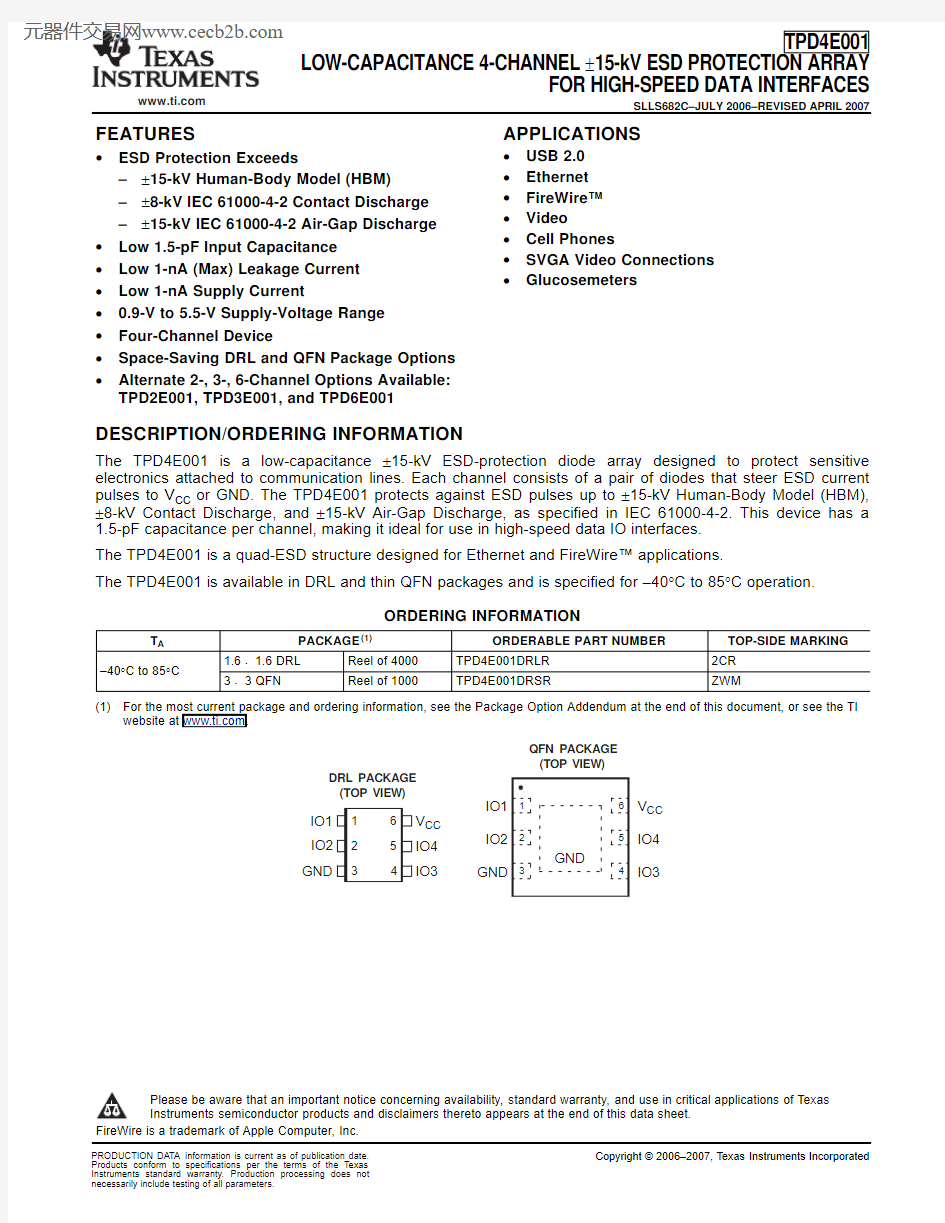
IO3
IO4V CC
QFN PACKAGE (TOP VIEW)
DRL PACKAGE (TOP VIEW)
IO3
IO4V CC TPD4E001
LOW-CAPACITANCE 4-CHANNEL ±15-kV ESD PROTECTION ARRAY
FOR HIGH-SPEED DATA INTERFACES
SLLS682C–JULY 2006–REVISED APRIL 2007
?USB 2.0?
ESD Protection Exceeds
?Ethernet –±15-kV Human-Body Model (HBM)
?FireWire?–±8-kV IEC 61000-4-2Contact Discharge ?Video
–±15-kV IEC 61000-4-2Air-Gap Discharge ?Cell Phones
?Low 1.5-pF Input Capacitance ?SVGA Video Connections ?Low 1-nA (Max)Leakage Current ?
Glucosemeters
?Low 1-nA Supply Current
?0.9-V to 5.5-V Supply-Voltage Range ?Four-Channel Device
?Space-Saving DRL and QFN Package Options ?
Alternate 2-,3-,6-Channel Options Available:TPD2E001,TPD3E001,and TPD6E001
The TPD4E001is a low-capacitance ±15-kV ESD-protection diode array designed to protect sensitive electronics attached to communication lines.Each channel consists of a pair of diodes that steer ESD current pulses to V CC or GND.The TPD4E001protects against ESD pulses up to ±15-kV Human-Body Model (HBM),±8-kV Contact Discharge,and ±15-kV Air-Gap Discharge,as specified in IEC 61000-4-2.This device has a 1.5-pF capacitance per channel,making it ideal for use in high-speed data IO interfaces.The TPD4E001is a quad-ESD structure designed for Ethernet and FireWire?applications.
The TPD4E001is available in DRL and thin QFN packages and is specified for –40°C to 85°C operation.
ORDERING INFORMATION
T A
PACKAGE (1)
ORDERABLE PART NUMBER TOP-SIDE MARKING 1.6×1.6DRL
Reel of 4000TPD4E001DRLR 2CR –40°C to 85°C 3×3QFN
Reel of 1000
TPD4E001DRSR
ZWM
(1)
For the most current package and ordering information,see the Package Option Addendum at the end of this document,or see the TI website at https://www.wendangku.net/doc/4c5242449.html, .
Please be aware that an important notice concerning availability,standard warranty,and use in critical applications of Texas Instruments semiconductor products and disclaimers thereto appears at the end of this data sheet.
元器件交易网https://www.wendangku.net/doc/4c5242449.html,
https://www.wendangku.net/doc/4c5242449.html,
Absolute Maximum Ratings (1)
TPD4E001
LOW-CAPACITANCE 4-CHANNEL ±15-kV ESD PROTECTION ARRAY
FOR HIGH-SPEED DATA INTERFACES
SLLS682C–JULY 2006–REVISED APRIL 2007
FUNCTIONAL BLOCK DIAGRAM
PIN DESCRIPTION
QFN/DRL https://www.wendangku.net/doc/4c5242449.html, FUNCTION
1,2,4,5
IOx ESD-protected channel 3GND Ground
6V CC Power-supply input.Bypass V CC to GND with a 0.1-μF ceramic capacitor.EP
EP
Exposed pad.Connect to GND.
over operating free-air temperature range (unless otherwise noted)
MIN
MAX
UNIT V CC –0.37
V V I/O –0.3V CC +0.3
V T stg Storage temperature range –65
150°C T J
Junction temperature 150°C Infrared (15s)220Bump temperature (soldering)°C Vapor phase (60s)
215Lead temperature (soldering,10s)
300
°C
(1)
Stresses beyond those listed under Absolute Maximum Ratings may cause permanent damage to the device.These are stress ratings only,and functional operation of the device at these or any other conditions beyond those indicated in the operational sections of the specifications is not implied.Exposure to absolute maximum rating conditions for extended periods may affect device reliability.
元器件交易网https://www.wendangku.net/doc/4c5242449.html,
https://www.wendangku.net/doc/4c5242449.html,
Electrical Characteristics ESD Protection
TPD4E001 LOW-CAPACITANCE4-CHANNEL±15-kV ESD PROTECTION ARRAY
FOR HIGH-SPEED DATA INTERFACES
SLLS682C–JULY2006–REVISED APRIL2007
V CC =5V±10%,T
A
=-40°C to85°C(unless otherwise noted)
PARAMETER TEST CONDITIONS MIN TYP(1)MAX UNIT
V CC Supply voltage0.9 5.5V
I CC Supply current1100nA
V F Diode forward voltage I F=10mA0.650.95V
V BR Breakdown Voltage I BR=10mA11V
Positive transients V CC+25
T A=25°C,±15-kV HBM,
I F=10A Negative transients–25
T A=25°C,Positive transients V CC+60
±8-kV Contact Discharge
V C Channel clamp voltage(2)V
Negative transients–60
(IEC61000-4-2),I F=24A
T A=25°C,Positive transients V CC+100
±15-kV Air-Gap Discharge
Negative transients–100
(IEC61000-4-2),I F=45A
I i/o Channel leakage current V i/o=GND to V CC±1nA
C i/o Channel input capacitance V CC=5V,Bias of V CC/2 1.5pF
(1)Typical values are at V CC=5V and T A=25°C.
(2)Channel clamp voltage is not production tested
PARAMETER TYP UNIT HBM±15kV
IEC61000-4-2Contact Discharge±8kV
IEC61000-4-2Air-Gap Discharge±15kV 元器件交易网https://www.wendangku.net/doc/4c5242449.html,
https://www.wendangku.net/doc/4c5242449.html,
TYPICAL OPERATING
CHARACTERISTICS
0.00
1.00
2.00
2.50
3.00
4.00
5.00
IO Voltage (V)
1.00
1.201.401.601.80
2.002.20I O C a p a c i t a n c e (p F
)
110
100
1000
–40
25
45
65
85
Temperature (°C)
I O L e a k a g e C u r r e n t (p A )
TPD4E001
LOW-CAPACITANCE 4-CHANNEL ±15-kV ESD PROTECTION ARRAY
FOR HIGH-SPEED DATA INTERFACES
SLLS682C–JULY 2006–REVISED APRIL 2007
IO CAPACITANCE
vs
IO VOLTAGE (V CC =5.0V)
IO LEAKAGE CURRENT
vs
TEMPERATURE (V CC =5.5V)
元器件交易网https://www.wendangku.net/doc/4c5242449.html,
https://www.wendangku.net/doc/4c5242449.html,
APPLICATION INFORMATION
Detailed Description
TPD4E001
LOW-CAPACITANCE 4-CHANNEL ±15-kV ESD PROTECTION ARRAY
FOR HIGH-SPEED DATA INTERFACES
SLLS682C–JULY 2006–REVISED APRIL 2007
When placed near the connector,the TPD4E001ESD solution offers little or no signal distortion during normal operation due to low IO capacitance and ultra-low leakage current specifications.The TPD4E001ensures that the core circuitry is protected and the system is functioning properly in the event of an ESD strike.For proper operation,the following layout/design guidelines should be followed:
1.Place the TPD4E001solution close to the connector.This allows the TPD4E001to take away the energy associated with ESD strike before it reaches the internal circuitry of the system board.
2.Place a 0.1-μF capacitor very close to the V CC pin.This limits any momentary voltage surge at the IO pin during the ESD strike event.
3.Ensure that there is enough metallization for the V CC and GND loop.During normal operation,the TPD4E001consumes nA leakage current.But during the ESD event,V CC and GND may see 15A to 30A of current,depending on the ESD level.Sufficient current path enables safe discharge of all the energy associated with the ESD strike.
4.Leave the unused IO pins floating .
5.The V CC pin can be connected in two different ways:
a.If the V CC pin is connected to the system power supply,the TPD4E001works as a transient suppressor
for any signal swing above V CC +V F .A 0.1-μF capacitor on the device V CC pin is recommended for ESD bypass.
b.If the V CC pin is not connected to the system power supply,the TPD4E001can tolerate higher signal
swing in the range up to 10V.Please note that a 0.1μF capacitor is still recommended at the V CC pin for ESD bypass.
元器件交易网https://www.wendangku.net/doc/4c5242449.html,
PACKAGING INFORMATION
Orderable Device Status (1)Package Type Package Drawing Pins Package Qty Eco Plan (2)
Lead/Ball Finish MSL Peak Temp (3)TPD4E001DRLR ACTIVE SOT-553DRL 64000Green (RoHS &
no Sb/Br)CU NIPDAU Level-1-260C-UNLIM TPD4E001DRLRG4
ACTIVE
SOT-553
DRL
6
4000Green (RoHS &
no Sb/Br)
CU NIPDAU
Level-1-260C-UNLIM
(1)
The marketing status values are defined as follows:ACTIVE:Product device recommended for new designs.
LIFEBUY:TI has announced that the device will be discontinued,and a lifetime-buy period is in effect.
NRND:Not recommended for new designs.Device is in production to support existing customers,but TI does not recommend using this part in a new design.
PREVIEW:Device has been announced but is not in production.Samples may or may not be available.OBSOLETE:TI has discontinued the production of the device.
(2)
Eco Plan -The planned eco-friendly classification:Pb-Free (RoHS),Pb-Free (RoHS Exempt),or Green (RoHS &no Sb/Br)-please check https://www.wendangku.net/doc/4c5242449.html,/productcontent for the latest availability information and additional product content details.TBD:The Pb-Free/Green conversion plan has not been defined.
Pb-Free (RoHS):TI's terms "Lead-Free"or "Pb-Free"mean semiconductor products that are compatible with the current RoHS requirements for all 6substances,including the requirement that lead not exceed 0.1%by weight in homogeneous materials.Where designed to be soldered at high temperatures,TI Pb-Free products are suitable for use in specified lead-free processes.
Pb-Free (RoHS Exempt):This component has a RoHS exemption for either 1)lead-based flip-chip solder bumps used between the die and package,or 2)lead-based die adhesive used between the die and leadframe.The component is otherwise considered Pb-Free (RoHS compatible)as defined above.
Green (RoHS &no Sb/Br):TI defines "Green"to mean Pb-Free (RoHS compatible),and free of Bromine (Br)and Antimony (Sb)based flame retardants (Br or Sb do not exceed 0.1%by weight in homogeneous material)
(3)
MSL,Peak Temp.--The Moisture Sensitivity Level rating according to the JEDEC industry standard classifications,and peak solder temperature.
Important Information and Disclaimer:The information provided on this page represents TI's knowledge and belief as of the date that it is provided.TI bases its knowledge and belief on information provided by third parties,and makes no representation or warranty as to the accuracy of such information.Efforts are underway to better integrate information from third parties.TI has taken and continues to take reasonable steps to provide representative and accurate information but
may not have conducted destructive testing or chemical analysis on incoming materials and chemicals.TI and TI suppliers consider certain information to be proprietary,and thus CAS numbers and other limited information may not be available for release.
In no event shall TI's liability arising out of such information exceed the total purchase price of the TI part(s)at issue in this document sold by TI to Customer on an annual basis.
PACKAGE OPTION ADDENDUM
https://www.wendangku.net/doc/4c5242449.html,
17-May-2007
TAPE AND REEL INFORMATION
Device Package Pins Site Reel
Diameter
(mm)
Reel
Width
(mm)
A0(mm)B0(mm)K0(mm)P1
(mm)
W
(mm)
Pin1
Quadrant
TPD4E001DRLR DRL6HNT1809 1.78 1.780.6948Q3
TAPE AND REEL BOX INFORMATION
Device Package Pins Site Length(mm)Width(mm)Height(mm) TPD4E001DRLR DRL6HNT201.0192.026.0
IMPORTANT NOTICE
Texas Instruments Incorporated and its subsidiaries(TI)reserve the right to make corrections,modifications,enhancements, improvements,and other changes to its products and services at any time and to discontinue any product or service without notice. Customers should obtain the latest relevant information before placing orders and should verify that such information is current and complete.All products are sold subject to TI’s terms and conditions of sale supplied at the time of order acknowledgment.
TI warrants performance of its hardware products to the specifications applicable at the time of sale in accordance with TI’s standard warranty.Testing and other quality control techniques are used to the extent TI deems necessary to support this warranty.Except where mandated by government requirements,testing of all parameters of each product is not necessarily performed.
TI assumes no liability for applications assistance or customer product design.Customers are responsible for their products and applications using TI components.To minimize the risks associated with customer products and applications,customers should provide adequate design and operating safeguards.
TI does not warrant or represent that any license,either express or implied,is granted under any TI patent right,copyright,mask work right,or other TI intellectual property right relating to any combination,machine,or process in which TI products or services are https://www.wendangku.net/doc/4c5242449.html,rmation published by TI regarding third-party products or services does not constitute a license from TI to use such products or services or a warranty or endorsement https://www.wendangku.net/doc/4c5242449.html,e of such information may require a license from a third party under the patents or other intellectual property of the third party,or a license from TI under the patents or other intellectual property of TI. Reproduction of TI information in TI data books or data sheets is permissible only if reproduction is without alteration and is accompanied by all associated warranties,conditions,limitations,and notices.Reproduction of this information with alteration is an unfair and deceptive business practice.TI is not responsible or liable for such altered https://www.wendangku.net/doc/4c5242449.html,rmation of third parties may be subject to additional restrictions.
Resale of TI products or services with statements different from or beyond the parameters stated by TI for that product or service voids all express and any implied warranties for the associated TI product or service and is an unfair and deceptive business practice.TI is not responsible or liable for any such statements.
TI products are not authorized for use in safety-critical applications(such as life support)where a failure of the TI product would reasonably be expected to cause severe personal injury or death,unless officers of the parties have executed an agreement specifically governing such use.Buyers represent that they have all necessary expertise in the safety and regulatory ramifications of their applications,and acknowledge and agree that they are solely responsible for all legal,regulatory and safety-related requirements concerning their products and any use of TI products in such safety-critical applications,notwithstanding any applications-related information or support that may be provided by TI.Further,Buyers must fully indemnify TI and its representatives against any damages arising out of the use of TI products in such safety-critical applications.
TI products are neither designed nor intended for use in military/aerospace applications or environments unless the TI products are specifically designated by TI as military-grade or"enhanced plastic."Only products designated by TI as military-grade meet military specifications.Buyers acknowledge and agree that any such use of TI products which TI has not designated as military-grade is solely at the Buyer's risk,and that they are solely responsible for compliance with all legal and regulatory requirements in connection with such use.
TI products are neither designed nor intended for use in automotive applications or environments unless the specific TI products are designated by TI as compliant with ISO/TS16949requirements.Buyers acknowledge and agree that,if they use any
non-designated products in automotive applications,TI will not be responsible for any failure to meet such requirements. Following are URLs where you can obtain information on other Texas Instruments products and application solutions:
Products Applications
Amplifiers Audio
Data Converters Automotive
DSP Broadband
Interface Digital Control
Logic Military
Power Mgmt Optical Networking
Microcontrollers Security
RFID Telephony
Low Power Video&Imaging
Wireless
Wireless
Mailing Address:Texas Instruments,Post Office Box655303,Dallas,Texas75265
Copyright?2007,Texas Instruments Incorporated