SN65HVD1050_08中文资料

FEATURES
DESCRIPTION
APPLICATIONS
FUNCTION BLOCK DIAGRAM
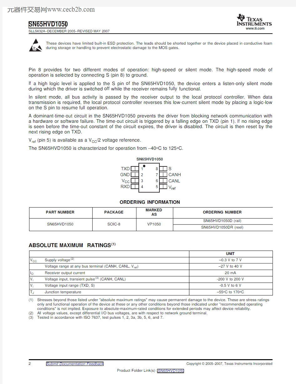
TXD
RXD
S
V ref CANH CANL
SN65HVD1050
SLLS632A–DECEMBER 2005–REVISED MAY 2007
https://www.wendangku.net/doc/4611354683.html,
EMC OPTIMIZED CAN TRANSCEIVER
?Improved Replacement for the TJA1050?High Electromagnetic Immunity (EMI)
The SN65HVD1050meets or exceeds the specifications of the ISO 11898standard for use in ?Very Low Electromagnetic Emissions (EME)applications employing a Controller Area Network ?
Meets or Exceeds the Requirements of (CAN).The device is also qualified for use in ISO 11898-2
automotive applications in accordance with
?Bus-Fault Protection of –27V to 40V AEC-Q100.
(1)
?Dominant Time-Out Function
As a CAN transceiver,this device provides differential transmit capability to the bus and differential receive ?
Power-Up/Down Glitch-Free Bus Inputs and capability to a CAN controller at signaling rates up to Outputs
1megabit per second (Mbps)(2).
–High Input Impedance with Low V CC
Designed for operation is especially harsh –Monotonic Outputs During Power Cycling
environments,the HVD1050features cross-wire,over-voltage and loss of ground protection from -27V to 40V,over-temperature shut down,a -12V to 12V ?Industrial Automation
common-mode range,and will withstand voltage –DeviceNet?Data Buses (Vendor ID #806)transients from -200V to 200V according to ISO 7637.
?SAE J2284High Speed CAN for Automotive Applications
(1)The device is available with Q100qualification as the SN65HVD1050Q (PRODUCT PREVIEW).
?SAE J1939Standard Data Bus Interface (2)
The signaling rate of a line is the number of voltage
?ISO 11783Standard Data Bus Interface transitions that are made per second expressed in the units ?
NMEA 2000Standard Data Bus Interface
bps (bits per second).
Please be aware that an important notice concerning availability,standard warranty,and use in critical applications of Texas Instruments semiconductor products and disclaimers thereto appears at the end of this data sheet.
https://www.wendangku.net/doc/4611354683.html,
V ref
ABSOLUTE MAXIMUM RATINGS (1)
SN65HVD1050
SLLS632A–DECEMBER 2005–REVISED MAY 2007
These devices have limited built-in ESD protection.The leads should be shorted together or the device placed in conductive foam during storage or handling to prevent electrostatic damage to the MOS gates.
Pin 8provides for two different modes of operation:high-speed or silent mode.The high-speed mode of operation is selected by connecting S (pin 8)to ground.
If a high logic level is applied to the S pin of the SN65HVD1050,the device enters a listen-only silent mode during which the driver is switched off while the receiver remains fully functional.
In silent mode,all bus activity is passed by the receiver output to the local protocol controller.When data transmission is required,the local protocol controller reverses this low-current silent mode by placing a logic-low on the S pin to resume full operation.
A dominant-time-out circuit in the SN65HVD1050prevents the driver from blocking network communication with a hardware or software failure.The time-out circuit is triggered by a falling edge on TXD (pin 1).If no rising edge is seen before the time-out constant of the circuit expires,the driver is disabled.The circuit is then reset by the next rising edge on TXD.
V ref (pin 5)is available as a V CC /2voltage reference.
The SN65HVD1050is characterized for operation from –40°C to 125°C.
ORDERING INFORMATION
MARKED PART NUMBER PACKAGE ORDERING NUMBER AS SN65HVD1050D (rail)SN65HVD1050
SOIC-8
VP1050
SN65HVD1050DR (reel)
UNIT
V CC Supply voltage (2)
–0.3V to 7V Voltage range at any bus terminal (CANH,CANL,V ref )–27V to 40V
I O Receiver output current
20mA V I Voltage input,transient pulse (3)(CANH,CANL)-200V to 200V V I Voltage input range (TXD,S)-0.5V to 6V T J Junction temperature
–55°C to 170°C
(1)Stresses beyond those listed under "absolute maximum ratings"may cause permanent damage to the device.These are stress ratings only and functional operation of the device at these or any other conditions beyond those indicated under "recommended operating conditions"is not implied.Exposure to absolute-maximum-rated conditions for extended periods may affect device reliability.(2)All voltage values,except differential I/O bus voltages,are with respect to network ground terminal.(3)
Tested in accordance with ISO 7637,test pulses 1,2,3a,3b,5,6,and 7.
https://www.wendangku.net/doc/4611354683.html,
ELECTROSTATIC DISCHARGE PROTECTION (1)
RECOMMENDED OPERATING CONDITIONS
SUPPLY CURRENT
DEVICE SWITCHING CHARACTERISTICS
DRIVER ELECTRICAL CHARACTERISTICS
SN65HVD1050
SLLS632A–DECEMBER 2005–REVISED MAY
2007
over operating free-air temperature range (unless otherwise noted)
PARAMETER
TEST CONDITIONS
VALUE IEC Contact Discharge IEC 61000-4-2
Bus terminals vs GND ±6kV Bus terminals vs GND ±8kV JEDEC Standard 22,Human Body Model Test Method A114-C.01All pins ±4kV Field-Induced-Charged JEDEC Standard 22,All pins
±1.5kV Device Model Test Method C101Machine Model ANSI/ESDS5.2-1996
±200V
(1)
All typical values at 25°C.
MIN
NOM
MAX UNIT V CC Supply voltage
4.75
5.25V V I or V IC Voltage at any bus terminal (separately or common mode)–1212V V IH High-level input voltage 2 5.25V TXD,S
V IL Low-level input voltage 00.8V V ID Differential input voltage –77
V Driver –70I OH High-level output current mA Receiver –2
Driver 70I OL Low-level output current mA Receiver
2See Thermal Characteristics table,1Mbps minimum T J
Junction temperature
–40
150
°C
signaling rate with R L =54?
over recommended operating conditions (unless otherwise noted)
PARAMETER
TEST CONDITIONS
MIN
TYP MAX UNIT
Silent mode
S at V CC ,V I =V CC
610I CC
5-V Supply current
Dominant V I =0V,60?Load,S at 0V 5070mA Recessive
V I =V CC ,No Load,S at 0V
6
10
over operating free-air temperature range (unless otherwise noted)
over recommended operating conditiions (unless otherwise noted)
https://www.wendangku.net/doc/4611354683.html,
DRIVER SWITCHING CHARACTERISTICS
RECEIVER ELECTRICAL CHARACTERISTICS
SN65HVD1050
SLLS632A–DECEMBER 2005–REVISED MAY 2007
DRIVER ELECTRICAL CHARACTERISTICS (continued)
over recommended operating conditiions
(unless otherwise noted)
over recommended operating conditions (unless otherwise noted)
over recommended operating conditions (unless otherwise noted)
https://www.wendangku.net/doc/4611354683.html,
RECEIVER SWITCHING CHARACTERISTICS
S-PIN CHARACTERISTICS
VREF-PIN CHARACTERISTICS
THERMAL CHARACTERISTICS
SN65HVD1050
SLLS632A–DECEMBER 2005–REVISED MAY 2007
RECEIVER ELECTRICAL CHARACTERISTICS (continued)
over recommended operating conditions (unless otherwise noted)
PARAMETER
TEST CONDITIONS
MIN TYP (1)
MAX UNIT
Input resistance matching
R I(m)
V (CANH)=V (CANL)
–3%
0%
3%
[1–(R IN (CANH)/R IN (CANL))]x 100%
over recommended operating conditiions (unless otherwise noted)
over recommended operating conditiions (unless otherwise noted)
PARAMETER
TEST CONDITIONS
MIN TYP MAX UNIT I IH High level input current S at 2V 204070μA
I IL
Low level input current
S at 0.8V
5
20
30
over operating free-air temperature range (unless otherwise noted)
PARAMETER
TEST CONDITIONS
MIN TYP
MAX
UNIT V O
Reference output voltage
–50μA
0.4V CC
0.5V CC 0.6V CC
V
over operating free-air temperature range (unless otherwise noted)
PARAMETER
TEST CONDITIONS
MIN TYP MAX UNIT
Low-K thermal resistance
(1)
211θJA Junction-to-Air
High-K thermal resistance
131Junction-to-Board Thermal °C/W
θJB 53Resistance
Junction-to-Case Thermal θJC
79Resistance
V CC =5.0V,T j =27°C,R L =60?,S at 0V,Input to TXD a 500kHz,50%duty cycle square wave.CL at 112
mW
RXD =15pF
P D
Average power dissipation
V CC =5.5V,T j =130°C,R L =45?,S at 0V,Input to TXD a 500kHz,50%duty cycle square wave.CL at 170
RXD =15pF
Junction temperature,thermal T J_shutdown 190
°C
shutdown (2)
(1)Tested in accordance with the Low-K or High-K thermal metric definitions of EIA/JESD51-3for leaded surface-mount packages.(2)
Extended operation in thermal shutdown may affect device reliability,see APPLICATIONS INFORMATION.
https://www.wendangku.net/doc/4611354683.html,
FUNCTION TABLES
PARAMETER MEASUREMENT INFORMATION
V O(CANH)
V O(CANL)
I 0
330 W +1%
?2 V 3 V TEST 3 7 V
SN65HVD1050
SLLS632A–DECEMBER 2005–REVISED MAY 2007
DRIVER
INPUTS
OUTPUTS
BUS STATE
TXD (1)
S
(1)
CANH
(1)
CANL
(1)
L L or Open
H L DOMINANT H X Z Z RECESSIVE Open X Z Z RECESSIVE X
H
Z
Z
RECESSIVE
(1)
H =high level;L =low level;X =irrelevant;?=indeterminate;Z =high impedance
RECEIVER
DIFFERENTIAL INPUTS OUTPUT RXD (1)
BUS STATE V ID =V(CANH)–V(CANL)
V ID ≥0.9V L DOMINANT
0.5V ??V ID ≤0.5V H RECESSIVE Open H RECESSIVE (1) H =high level;L =low level;X =irrelevant;?=indeterminate;Z =high impedance Figure 1.Driver Voltage,Current,and Test Definition Figure 2.Bus Logic State Voltage Definitions Figure 3.Driver V OD Test Circuit https://www.wendangku.net/doc/4611354683.html, V I (CANH)+ V I (CANL) 2 V IC = V I V I O 3.5 V 1.5 V V OH V OL SN65HVD1050 SLLS632A–DECEMBER 2005–REVISED MAY 2007 PARAMETER MEASUREMENT INFORMATION (continued) Figure 4.Driver Test Circuit and Voltage Waveforms Figure 5.Receiver Voltage and Current Definitions A.The input pulse is supplied by a generator having the following characteristics:PRR ≤125kHz,50%duty cycle,t r ≤6ns,t f ≤6ns,Z O =50?. B. C L includes instrumentation and fixture capacitance within 20%. Figure 6.Receiver Test Circuit and Voltage Waveforms Table 1.Differential Input Voltage Threshold Test INPUT OUTPUT V CANH V CANL |V ID |R –11.1V –12V 900mV L V OL 12V 11.1V 900mV L –6V –12V 6V L 12V 6V 6V L –11.5V –12V 500mV H V OH 12V 11.5V 500mV H –12V –6V 6V H 6V 12V 6V H Open Open X H https://www.wendangku.net/doc/4611354683.html, 60 W +1% V CC 0 V V OH V OL NOTE: All V I input pulses are supplied by a generator having the following characteristics: t r or t f ≤ 6 ns, Pulse Repetition Rate (PRR) = 25 kHz, 50% duty cycle V I V O(CANH) + V O(CANL)2 V V CC 0 V V OH V OL 60±1% W SN65HVD1050 SLLS632A–DECEMBER 2005–REVISED MAY 2007 Figure 7.t en Test Circuit and Waveform NOTE:All V I input pulses are from 0V to V CC and supplied by a generator having the following characteristics:t r or t f ≤6ns. Pulse Repetition Rate (PRR)=125kHz,50%duty cycle. Figure https://www.wendangku.net/doc/4611354683.html,mon Mode Output Voltage Test and Waveforms A. All V I input pulses are from 0V to V CC and supplied by a generator having the following characteristics:t r or t f ≤6ns.Pulse Repetition Rate (PRR)=125kHz,50%duty cycle. Figure 9.t (LOOP)Test Circuit and Waveform https://www.wendangku.net/doc/4611354683.html, V I V OD V CC 0 V V OD(D) 0 V 12 V ?12 V ?12 V or 12 V | I OS(SS)| SN65HVD1050 SLLS632A–DECEMBER2005–REVISED MAY2007 A.All V I input pulses are from0V to V CC and supplied by a generator having the following characteristics:t r or t f≤6ns. Pulse Repetition Rate(PRR)=500Hz,50%duty cycle. B.C L=100pF includes instrumentation and fixture capacitance within±20%. Figure10.Dominant Time-Out Test Circuit and Waveforms Figure11.Driver Short-Circuit Current Test and Waveform https://www.wendangku.net/doc/4611354683.html, DEVICE INFORMATION SN65HVD1050 SLLS632A–DECEMBER 2005–REVISED MAY 2007 Table 2.Parametric Cross Reference With the TJA1050 TJA1050(1)PARAMETER HVD1050 TRANSMITTER SECTION V IH High-level input voltage Recommended V IH V IL Low-level input voltage Recommended V IL I IH High-level input current Driver I IH I IL Low-level input current Driver I IL BUS SECTION I LI Power-off bus input current Receiver I I(off)I O(SC)Short-circuit output current Driver I OS(SS)V O(dom)Dominant output voltage Driver V O(D) V i(dif)(th)Differential input voltage Receiver V IT and recommended V ID V i(dif)(hys)Diffrential input hysteresis Receiver V hys V O(reces)Recessive output voltage Driver V O(R) V O(dif)(bus)Differential bus voltage Driver V OD(D)and V OD(R)R i(cm)CANH,CANL input resistance Receiver R IN R i(dif)Differential input resistance Receiver R ID R i(cm)(m)Input resistance matching Receiver R I (m)C i Input capacitance to ground Receiver C I C i(dif)Differential input capacitance Receiver C ID RECEIVER SECTION I OH High-level output current Recommended I OH I OL Low-level output current Recommended I OL Vref PIN SECTION V ref Reference output voltage V O TIMING SECTION t d(TXD-BUSon)Delay TXD to bus active Driver t PLH t d(TXD-BUSoff)Delay TXD to bus inactive Driver t PHL t d(BUSon-RXD)Delay bus active to RXD Receiver t PHL t d(BUSoff-RXD) Delay bus inactive to RXD Receiver t PLH t d(TXD-BUSon)+t d(BUSon-RXD)Device t LOOP1t d(TXD-BUSoff)+t d(BUSoff-RXD) Device t LOOP2t dom(TXD)Dominant time out Driver t (dom) S PIN SECTION V IH High-level input voltage Recommended V IH V IL Low-level input voltage Recommended V IL I IH High-level input current I IH I IL Low-level input current I IL (1) From TJA1050Product Specification,Philips Semiconductors,2002May 16. https://www.wendangku.net/doc/4611354683.html, Equivalent Input and Output Schematic Diagrams SN65HVD1050 SLLS632A–DECEMBER 2005–REVISED MAY 2007 https://www.wendangku.net/doc/4611354683.html, TYPICAL CHARACTERISTICS ?40 02570125 ?R e c e s s i v e -t o -D o m i n a n t L o o p T i m e ?n s t L O O P 1T A ?Free-Air T emperature ?°C 140 145 150 155 160 165 170 ?4002570125 ?D o m i n a n t -t o -R e c e s s i v e L o o p T i m e ?n s t L O O P 2T A ?Free-Air T emperature ?°C ?10 1020304050607080900 12345 I O L ? L o w -L e v e l O u t p u t C u r r e n t ? m A V O CANL ? Low-Level Output Voltage ? V 51015202530354045 50Signaling Rate ? kbps I C C ? R M S S u p p l y C u r r e n t ? m A SN65HVD1050 SLLS632A–DECEMBER 2005–REVISED MAY 2007 RECESSIVE-TO-DOMINANT LOOP TIME DOMINANT-TO-RECESSIVE LOOP TIME vs vs FREE-AIR TEMPERATURE (across V CC ) FREE-AIR TEMPERATURE (across V CC ) Figure 12. Figure 13. SUPPLY CURRENT (RMS) DRIVER LOW-LEVEL OUTPUT VOLTAGE vs vs SIGNALING RATE LOW-LEVEL OUTPUT CURRENT Figure 14. Figure 15. https://www.wendangku.net/doc/4611354683.html, -0 -10-20-30-40-50-60-70-80 01234 5I O H ?H i g h -L e v e l O u t p u t C u r r e n t ?m A V O CANH ?High-Level Output V oltage ?V 0.5 1 1.5 2 2.5 3 ?40 02570125 T A ? Free-Air Temperature ? °C D o m i n a n t D r i v e r D i f f e r e n t i a l O u t p u t V o l t a g e ? V I O ? D i f f e r e n t i a l D r i v e r O u t p u t C u r r e n t ? m A V CC ? Supply Voltage ? V 0.60.60.70.70.80.80.80.80.70.70.60.6? R e c e i v e r O u t p u t V o l t a g e ? V V O V ID ? Differential Input Voltage ? V SN65HVD1050 SLLS632A–DECEMBER 2005–REVISED MAY 2007 TYPICAL CHARACTERISTICS (continued) DRIVER HIGH-LEVEL OUTPUT VOLTAGE DRIVER DIFFERENTIAL OUTPUT VOLTAGE vs vs HIGH-LEVEL OUTPUT CURRENT FREE-AIR TEMPERATURE (across V CC ) Figure 16. Figure 17. DRIVER OUTPUT CURRENT RECEIVER OUTPUT VOLTAGE vs vs SUPPLY VOLTAGE DIFFERENTIAL INPUT VOLTAGE Figure 18. Figure 19. https://www.wendangku.net/doc/4611354683.html, D B V m 020 40 60 80 0.1 1 10 1001000 f ? Frequency ? MHz d B m SN65HVD1050 SLLS632A–DECEMBER 2005–REVISED MAY 2007 TYPICAL CHARACTERISTICS (continued) TYPICAL ELECTROMAGNETIC EMISSIONS TYPICAL ELECTROMAGNETIC UP TO 50MHZ (Peak Amplitude) IMMUNITY PERFORMANCE Figure 20.Frequency Spectrum of Common-Mode Figure 21.Direct Power Injection (DPI)Response vs Emissions Frequency https://www.wendangku.net/doc/4611354683.html, APPLICATION INFORMATION THERMAL SHUTDOWN SN65HVD1050 SLLS632A–DECEMBER2005–REVISED MAY2007 The SN65HVD1050has a thermal shutdown feature that turns off the driver outputs when the junction temperature nears190°C.This shutdown prevents catastrophic failure from bus shorts,but does not protect the circuit from possible damage.The user should strive to maintain recommended operating conditions and not exceed absolute-maximum ratings at all times.If an SN65HVD1050is subjected to many,or long-duration faults that can put the device into thermal shutdown,it should be replaced. PACKAGING INFORMATION Orderable Device Status (1)Package Type Package Drawing Pins Package Qty Eco Plan (2) Lead/Ball Finish MSL Peak Temp (3)SN65HVD1050D ACTIVE SOIC D 875Green (RoHS &no Sb/Br)CU NIPDAU Level-1-260C-UNLIM SN65HVD1050DG4ACTIVE SOIC D 875 Green (RoHS &no Sb/Br) CU NIPDAU Level-1-260C-UNLIM SN65HVD1050DR ACTIVE SOIC D 82500Green (RoHS & no Sb/Br)CU NIPDAU Level-1-260C-UNLIM SN65HVD1050DRG4 ACTIVE SOIC D 8 2500Green (RoHS & no Sb/Br) CU NIPDAU Level-1-260C-UNLIM (1) The marketing status values are defined as follows:ACTIVE:Product device recommended for new designs. LIFEBUY:TI has announced that the device will be discontinued,and a lifetime-buy period is in effect. NRND:Not recommended for new designs.Device is in production to support existing customers,but TI does not recommend using this part in a new design. PREVIEW:Device has been announced but is not in production.Samples may or may not be available.OBSOLETE:TI has discontinued the production of the device. (2) Eco Plan -The planned eco-friendly classification:Pb-Free (RoHS),Pb-Free (RoHS Exempt),or Green (RoHS &no Sb/Br)-please check https://www.wendangku.net/doc/4611354683.html,/productcontent for the latest availability information and additional product content details.TBD:The Pb-Free/Green conversion plan has not been defined. Pb-Free (RoHS):TI's terms "Lead-Free"or "Pb-Free"mean semiconductor products that are compatible with the current RoHS requirements for all 6substances,including the requirement that lead not exceed 0.1%by weight in homogeneous materials.Where designed to be soldered at high temperatures,TI Pb-Free products are suitable for use in specified lead-free processes. Pb-Free (RoHS Exempt):This component has a RoHS exemption for either 1)lead-based flip-chip solder bumps used between the die and package,or 2)lead-based die adhesive used between the die and leadframe.The component is otherwise considered Pb-Free (RoHS compatible)as defined above. Green (RoHS &no Sb/Br):TI defines "Green"to mean Pb-Free (RoHS compatible),and free of Bromine (Br)and Antimony (Sb)based flame retardants (Br or Sb do not exceed 0.1%by weight in homogeneous material) (3) MSL,Peak Temp.--The Moisture Sensitivity Level rating according to the JEDEC industry standard classifications,and peak solder temperature. Important Information and Disclaimer:The information provided on this page represents TI's knowledge and belief as of the date that it is provided.TI bases its knowledge and belief on information provided by third parties,and makes no representation or warranty as to the accuracy of such information.Efforts are underway to better integrate information from third parties.TI has taken and continues to take reasonable steps to provide representative and accurate information but may not have conducted destructive testing or chemical analysis on incoming materials and chemicals.TI and TI suppliers consider certain information to be proprietary,and thus CAS numbers and other limited information may not be available for release. In no event shall TI's liability arising out of such information exceed the total purchase price of the TI part(s)at issue in this document sold by TI to Customer on an annual basis. PACKAGE OPTION ADDENDUM https://www.wendangku.net/doc/4611354683.html, 26-Apr-2007 TAPE AND REEL INFORMATION *All dimensions are nominal Device Package Type Package Drawing Pins SPQ Reel Diameter (mm)Reel Width W1(mm)A0(mm)B0(mm)K0(mm) P1(mm)W (mm)Pin1Quadrant SN65HVD1050DR SOIC D 8 2500330.0 12.4 6.4 5.2 2.1 8.0 12.0 Q1 *All dimensions are nominal Device Package Type Package Drawing Pins SPQ Length(mm)Width(mm)Height(mm) SN65HVD1050DR SOIC D8*******.0346.029.0 IMPORTANT NOTICE Texas Instruments Incorporated and its subsidiaries(TI)reserve the right to make corrections,modifications,enhancements,improvements, and other changes to its products and services at any time and to discontinue any product or service without notice.Customers should obtain the latest relevant information before placing orders and should verify that such information is current and complete.All products are sold subject to TI’s terms and conditions of sale supplied at the time of order acknowledgment. TI warrants performance of its hardware products to the specifications applicable at the time of sale in accordance with TI’s standard warranty.Testing and other quality control techniques are used to the extent TI deems necessary to support this warranty.Except where mandated by government requirements,testing of all parameters of each product is not necessarily performed. TI assumes no liability for applications assistance or customer product design.Customers are responsible for their products and applications using TI components.To minimize the risks associated with customer products and applications,customers should provide adequate design and operating safeguards. TI does not warrant or represent that any license,either express or implied,is granted under any TI patent right,copyright,mask work right, or other TI intellectual property right relating to any combination,machine,or process in which TI products or services are https://www.wendangku.net/doc/4611354683.html,rmation published by TI regarding third-party products or services does not constitute a license from TI to use such products or services or a warranty or endorsement https://www.wendangku.net/doc/4611354683.html,e of such information may require a license from a third party under the patents or other intellectual property of the third party,or a license from TI under the patents or other intellectual property of TI. Reproduction of TI information in TI data books or data sheets is permissible only if reproduction is without alteration and is accompanied by all associated warranties,conditions,limitations,and notices.Reproduction of this information with alteration is an unfair and deceptive business practice.TI is not responsible or liable for such altered https://www.wendangku.net/doc/4611354683.html,rmation of third parties may be subject to additional restrictions. Resale of TI products or services with statements different from or beyond the parameters stated by TI for that product or service voids all express and any implied warranties for the associated TI product or service and is an unfair and deceptive business practice.TI is not responsible or liable for any such statements. TI products are not authorized for use in safety-critical applications(such as life support)where a failure of the TI product would reasonably be expected to cause severe personal injury or death,unless officers of the parties have executed an agreement specifically governing such use.Buyers represent that they have all necessary expertise in the safety and regulatory ramifications of their applications,and acknowledge and agree that they are solely responsible for all legal,regulatory and safety-related requirements concerning their products and any use of TI products in such safety-critical applications,notwithstanding any applications-related information or support that may be provided by TI.Further,Buyers must fully indemnify TI and its representatives against any damages arising out of the use of TI products in such safety-critical applications. TI products are neither designed nor intended for use in military/aerospace applications or environments unless the TI products are specifically designated by TI as military-grade or"enhanced plastic."Only products designated by TI as military-grade meet military specifications.Buyers acknowledge and agree that any such use of TI products which TI has not designated as military-grade is solely at the Buyer's risk,and that they are solely responsible for compliance with all legal and regulatory requirements in connection with such use. TI products are neither designed nor intended for use in automotive applications or environments unless the specific TI products are designated by TI as compliant with ISO/TS16949requirements.Buyers acknowledge and agree that,if they use any non-designated products in automotive applications,TI will not be responsible for any failure to meet such requirements. Following are URLs where you can obtain information on other Texas Instruments products and application solutions: Products Applications Amplifiers Audio Data Converters Automotive DSP Broadband Clocks and Timers Digital Control Interface Medical Logic Military Power Mgmt Optical Networking Microcontrollers Security RFID Telephony RF/IF and ZigBee?Solutions Video&Imaging Wireless Mailing Address:Texas Instruments,Post Office Box655303,Dallas,Texas75265 Copyright?2008,Texas Instruments Incorporated