FAN4800A中文资料

Features
Pin-to-Pin Compatible with ML4800 and FAN4800 and CM6800 and CM6800A
PWM Configurable for Current-mode or
Feed-forward Voltage-Mode Operation
Internally Synchronized Leading-Edge PFC and Trailing-Edge PWM in one IC
Low Operating Current
Innovative Switching-Charge Multiplier Divider
Average-Current-Mode for Input-Current Shaping PFC Over-Voltage and Under-Voltage Protections PFC Feedback Open-Loop Protection
Cycle-by-Cycle Current Limiting for PFC/PWM
Power-on Sequence Control and Soft-Start
Brownout Protection
Interleaved PFC/PWM Switching
FAN4801/1S/2/2L Improve Efficiency at Light Load f RTCT=4?f PFC=4?f PWM for FAN4800A and
FAN4801/1S
f RTCT=4?f PFC=2?f PWM for FAN4800C and
FAN4802/2L
Applications
Desktop PC Power Supply
Internet Server Power Supply
LCD TV, Monitor Power Supply
UPS
Battery Charger
DC Motor Power Supply
Monitor Power Supply Description
The highly integrated FAN4800A/C and FAN4801/1S/2/2L are specially designed for power supplies that consist of boost PFC and PWM. They require very few external components to achieve versatile protections / compensation. They are available
in 16-pin DIP and SOP packages.
The PWM can be used in either current or voltage mode. In voltage mode, feed-forward from the PFC output bus can reduce the secondary output ripple. Compared with older productions, ML4800 and FAN4800, FAN4800A/C and FAN4801/1S/2/2L have lower operation current that save power consumption in external devices. FAN4800A/C and FAN4801/1S/2/2L have accurate 49.9% maximum duty of PWM that makes the hold-up time longer. Specifically, the brownout protection and PFC soft-start functions are not
in ML4800 and FAN4800.
To start evaluating FAN4800A/C, FAN4801/1S/2/2L for replacing existing FAN4800 and ML4800 boards, five things must be done before the fine-tuning procedure:
1. Change R AC resister from the old value to a higher
resister: between 6MΩ to 8MΩ.
2. Change RT/CT pin from the existing values to
R T=6.8KΩ and C T=1000pF to have f PFC=64KHz,
f PWM=64KHz.
3. VRMS pin needs to be 1.224V at V IN=85 V AC for
universal input application from line input from
85V AC to 270 V AC. Both poles for the V rms of
FAN4801/1S/2/2L don’t need to substantially
slower than FAN4800; about 5 to 10 times.
4. At full load, the average V EA needs to ~4.5V and
the ripple on the V EA needs to be less than 400mV.
5. Soft-Start pin, the soft-start current has been
reduced to half from the FAN4800 capacitor. Related Resources
FAN4800A/C, FAN4801/1S/2/2L — PFC/PWM Controller Combination
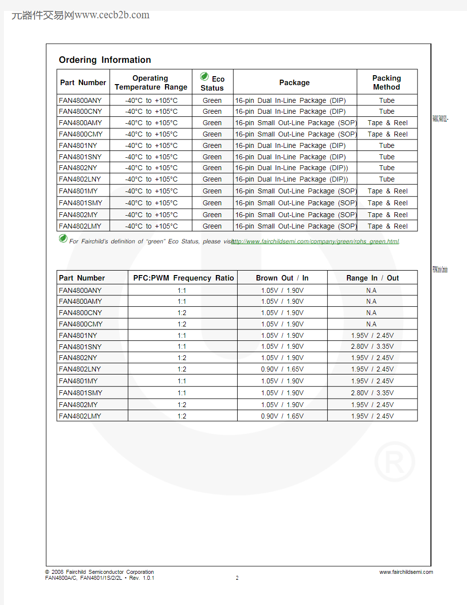
FAN4800AMY -40°C to +105°C Green 16-pin Small Out-Line Package (SOP) Tape & Reel FAN4800CMY -40°C to +105°C Green 16-pin Small Out-Line Package (SOP) Tape & Reel
FAN4801NY -40°C to +105°C Green 16-pin Dual In-Line Package (DIP) Tube FAN4801SNY -40°C to +105°C Green 16-pin Dual In-Line Package (DIP) Tube FAN4802NY -40°C to +105°C Green 16-pin Dual In-Line Package (DIP)) Tube FAN4802LNY -40°C to +105°C Green 16-pin Dual In-Line Package (DIP)) Tube FAN4801MY -40°C to +105°C Green 16-pin Small Out-Line Package (SOP) Tape & Reel FAN4801SMY -40°C to +105°C Green 16-pin Small Out-Line Package (SOP) Tape & Reel FAN4802MY -40°C to +105°C Green 16-pin Small Out-Line Package (SOP) Tape & Reel FAN4802LMY
-40°C to +105°C
Green
16-pin Small Out-Line Package (SOP)
Tape & Reel
For Fairchild’s definition of “green” Eco Status, please visit: https://www.wendangku.net/doc/5b3159045.html,/company/green/rohs_green.html .
Part Number
PFC:PWM Frequency Ratio
Brown Out / In
Range In / Out
FAN4800ANY 1:1 1.05V / 1.90V N.A FAN4800AMY 1:1 1.05V / 1.90V N.A FAN4800CNY 1:2 1.05V / 1.90V N.A FAN4800CMY 1:2 1.05V / 1.90V N.A FAN4801NY 1:1 1.05V / 1.90V 1.95V / 2.45V FAN4801SNY 1:1 1.05V / 1.90V 2.80V / 3.35V FAN4802NY 1:2 1.05V / 1.90V 1.95V / 2.45V FAN4802LNY 1:2 0.90V / 1.65V 1.95V / 2.45V FAN4801MY 1:1 1.05V / 1.90V 1.95V / 2.45V FAN4801SMY 1:1 1.05V / 1.90V 2.80V / 3.35V FAN4802MY 1:2 1.05V / 1.90V 1.95V / 2.45V FAN4802LMY
1:2
0.90V / 1.65V
1.95V /
2.45V
PFC/PWM Controller Combination
IEA RAMP
RT/CT FBPWM SS VRMS ISENSE IAC ILIMIT
GND OPWM OPFC VDD VREF
FBPFC VEA FAN4800A/C FAN4801/1S/2/2L
VDD
VREF
Secondary
Figure 1.
Typical Application Current Mode
PFC/PWM Controller Combination
IEA RAMP
RT/CT FBPWM SS VRMS ISENSE IAC ILIMIT
GND OPWM OPFC VDD VREF
FBPFC VEA FAN4800A/C FAN4801/1S/2/2L VDD
VREF
Secondary
VREF
Figure 2.
Typical Application Voltage Mode
PFC/PWM Controller Combination
Figure 3. FAN4800A/C Function Block Diagram
PFC/PWM Controller Combination
Figure 5. F – Fairchild logo Z – Plant code
X – 1 digit year code Y – 1 digit week code
TT – 2 digits die run code
T – Package type (N:DIP, M:SOP)P – Y: Green package
M – Manufacture flow code
PFC/PWM Controller Combination
Figure 6. Pin Configuration (Top View )
Pin Definitions
Pin #
Name
Description
1 IEA
Output of PFC Current Amplifier. The signal from this pin is compared with an internal
sawtooth to determine the pulse width for PFC gate drive. 2 IAC
Input AC Current. For normal operation, this input provides current reference for the multiplier.
The suggested maximum IAC is 100μA. 3 ISENSE
PFC Current Sense. The non-inverting input of the PFC current amplifier and the output of
multiplier and PFC ILIMIT comparator. 4 VRMS Line-Voltage Detection. Line voltage detection. The pin is used for PFC multiplier.
5 SS PWM Soft-Start. During startup, the SS pin charges an external capacitor with a 10μA constant current source. The voltage on FBPWM is clamped by SS during startup. In the event
of a protection condition occurring and/or PWM disabled, the SS pin is quickly discharged. 6 FBPWM PWM Feedback Input. The control input for voltage-loop feedback of PWM stage. 7 RT/CT Oscillator RC Timing Connection. Oscillator timing node; timing set by R T and C T . 8 RAMP
PWM RAMP Input. In current mode, this pin functions as the current sense input; when in voltage mode, it is the feed forward sense input from PFC output 380V (feedforward ramp). 9 ILIMIT Peak Current Limit Setting for PWM. The peak current limits setting for PWM. 10 GND Ground.
11 OPWM
PWM Gate Drive. The totem-pole output drive for PWM MOSFET. This pin is internally clamped under 15V to protect the MOSFET. 12 OPFC
PFC Gate Drive. The totem pole output drive for PWM MOSFET. This pin is internally clamped
under 15V to protect the MOSFET. 13 VDD
Supply. The power supply pin. The threshold voltages for startup and turn-off are 11V and
9.3V, respectively. The operating current is lower than 10mA.
FAN4800A/C, FAN4801/1S/2/2L — PFC/PWM Controller Combination
Symbol Parameter
Min. Max. Unit
V DD DC Supply Voltage
30 V V H SS, FBPWM, RAMP, OPWM, OPFC -0.3 30.0 V V L
IAC, VRMS, RT/CT, ILIMIT, FBPFC, VEA
-0.3 7.0 V V VREF VREF 7.5 V V IEA IEA 0 V VREF +0.3 V
V N ISENSE -5.0 0.7 V I AC Input AC Current 1 mA I REF VREF Output Current
5 mA I PFC-OUT Peak PFC OUT Current, Source or Sink 0.5 A I PWM-OUT Peak PWM OUT Current, Source or Sink 0.5 A P D Power Dissipation T A < 50°C
800
mW
DIP 80.80 °C/W R Θ j-a Thermal Resistance (Junction to Air) SOP 104.10 °C/W
T J Operating Junction Temperature -40 +125 °C T STG Storage Temperature Range -55 +150 °C T L Lead Temperature (Soldering)
+260 °C Human Body Model
4.5 kV ESD
Electrostatic Discharge Capability Charged Device Model
1000
V
Notes:
1. All voltage values, except differential voltage, are given with respect to GND pin.
2. Stresses beyond those listed under “absolute maximum ratings “may cause permanent damage to the device.
Recommended Operating Conditions
The Recommended Operating Conditions table defines the conditions for actual device operation. Recommended operating conditions are specified to ensure optimal performance to the datasheet specifications. Fairchild does not recommend exceeding them or designing to Absolute Maximum Ratings.
Symbol Parameter Min. Typ. Max. Unit
T A
Operating Ambient Temperature
-40
+105
°C
PFC/PWM Controller Combination
Oscillator
f OSC-RT/CT RT/CT Frequency
R T=6.8k ?, C T=1000pF 240 256 268 kHz PFC & PWM Frequency
60
64
67
f OSC
FAN4800C,FAN4802/02L PWM Frequency
R T=6.8k ?, C T=1000pF 120 128 134
kHz f DV Voltage Stability 11V ≦ V DD ≦ 22V 2 % f DT Temperature Stability -40°C ~ +105°C
2
%
f TV
Total Variation (PFC &
PWM)(1)
Line, Temperature 58 70 kHz f RV Ramp Voltage (1)
Valley to Peak
2.8
V
I Discharge Discharge Current V RAMP =0V, V RT/CT =
2.5V 6.5 15.0 mA
f RANGE Frequency Range (1)
50 75 kHz t PFCD PFC Dead Time
R T=6.8k ?, C T=1000pF
400 600 800 ns
VREF
V VREF Reference Voltage I REF =0mA, C REF 0.1μF 7.4 7.5 7.6 V ΔV VREF1 Load Regulation of
Reference Voltage C REF =0.1μF, I REF =0mA to 3.5mA
V VDD =14V, Rise/Fall Time > 20μs 30 50 mV ΔV VREF2 Line Regulation of Reference Voltage C REF =0.1μF, V VDD =11V to 22V 25 mV ΔV VREF-DT (1)
Temperature Stability -40°C ~ +105°C 0.4 0.5 % ΔV VREF-TV (1)
Total Variation Line, Load, Temp 7.35 7.65 V ΔV VREF-LS
(1)
Long-Term Stability T J =125°C, 0 ~ 1000HRs 5 25 mV I REF-MAX . Maximum Current V VREF > 7.35V 5 mA I OS
(1)
Output Short Circuit
25
mA
PFC OVP Comparator
V PFC-OVP Over-Voltage Protection 2.70 2.75 2.80 V
PFC/PWM Controller Combination
=
=V VEA-H Output High Voltage on
V VEA
5.8 6 V V VEA-L
Output Low Voltage on V VEA
0.1 0.4 V
Current Error Amplifier V ISENSE
Input Voltage Range
(ISENSE pin)(1)
-1.5 0.7 V Gm I Transconductance
V NONINV =V INV , V IEA =3.75V 78 88 100 μmho V OFFSET Input Offset Voltage V VEA =0V, IAC Open
-10
10
mV
V IEA-H
Output High Voltage
6.8
7.4
8.0 V
V IEA-L Output Low Voltage 0.1 0.4 V
I L Source Current V ISENSE =-0.6V, V IEA =
1.5V 35 50 μA I H Sink Current V ISENSE =+0.6V, V IEA = 4.0V -50 -35 μA
A I Open-Loop Gain
(1)
40 50 dB Tri-Fault Detect t FBPFC_OPEN Time to FBPFC Open (1)
V FBPFC =V PFC-UVP to FBPFC OPEN,
470pF from FBPFC to GND
2 4 ms
V PFC-UVP
PFC Feedback Under-Voltage Protection 0.4 0.5 0.6 V
Gain Modulator
I AC
Input for AC Current (1)
Multiplier Linear Range 0 100 μA
I AC=17.67μA, V RMS=1.080V
V FBPFC=2.25V, at T=25°C
7.50 9.00 10.50 I AC=20μA, V RMS=1.224V V FBPFC =2.25V, at T=25°C
6.30
7.00 7.70 I AC=25.69μA, V RMS=1.585V
V FBPFC=2.25V, at T=25°C 3.80 4.20 4.60 I 51.62μA, V 3.169V GAIN GAIN Modulator (2)
PFC/PWM Controller Combination
=V GATE-L Gate Low Voltage V DD =15V; I O =100mA 1.5 V V GATE-H Gate High Voltage V DD =13V; I O =
100mA 8 V
t r Gate Rising Time V DD =15V; C L =4.7nF; O/P=2V to 9V 40 70 120 ns t f Gate Falling Time V DD =15V; C L =4.7nF; O/P=9V to 2V
40
60
110
ns
D PFC-MAX Maximum Duty Cycle V IEA <1.2V 94 97 %
D PFC-MIN Minimum Duty Cycle
V IEA >4.5V 0 %
Brown Out FAN4800A/C, FAN4801/1S/2 1.00 1.05 1.10 V V RMS-UVP
VRMS Threshold Low
FAN4802L 0.85 0.90 0.95 V
FAN4800A/C, FAN4801/1S/2 1.85 1.90 1.95 V
V RMS-UVP VRMS Threshold High
FAN4802L 1.60 1.65 1.70 V FAN4800A/C, FAN4801/1S/2
750
850
950
mV
ΔV RMS-UVP Hysteresis
FAN4802L 650 750 850 mV
t UVP Under-Voltage
Protection Delay Time
340 410 480 ms
Soft Start
V SS-MAX Maximum Voltage V DD 15V 9.5 10.0 10.5 V
I SS Soft-Start Current
10 μA
PWM ILIMIT Comparator V PWM-ILIMIT
Threshold Voltage 0.95 1.00 1.05 V t PD Delay to Output
250 ns
t PWM-Bnk
Leading-Edge Blanking
Time
170 250 350 ns
Range (FAN4801/1S/2/2L)
V RMS-L RMS AC Voltage Low When V RMS =1.95V at132Vrms 1.90 1.95 2.00 V
PFC/PWM Controller Combination
=
=
===Notes:
3. This parameter, although guaranteed by design, is not 100% production tested.
4. Gain=K ×
5.3 × (VRMS 2)-1; K=( ISENSE - I OFFSET ) × [IAC × (VEA - 0.7V)]-1
; VEA (MAX.)=5.6V.
PFC/PWM Controller Combination
10.8
10.911.0
11.1
11.211.311.4
-40℃-25℃-10℃
5℃
20℃
35℃
50℃
65℃
80℃
95℃110℃125℃
V T H -O N (V )
1.3
1.41.51.61.71.81.9
2.0-40℃-25℃-10℃5℃20℃35℃50℃65℃80℃95℃110℃125℃
△V T H (V )
Figure 9. V TH-ON vs. Temperature
Figure 10. ΔV TH vs. Temperature
27.86
27.8827.9027.9227.9427.9627.9828.00
28.0228.04-40℃-25℃-10℃
5℃
20℃
35℃
50℃
65℃
80℃
95℃
110℃125℃
V D D -O V P (V )
64.2
64.364.464.564.664.764.8
64.965.0-40℃
-25℃-10℃5℃20℃35℃50℃65℃80℃95℃110℃125℃
F O S C -F A N 4801/1S (k H z )
Figure 11. V DD-OVP vs. Temperature
Figure 12. f OSC-FAN4801/1S vs. Temperature
129.8130.0650655
PFC/PWM Controller Combination
-0.02
0.000.020.040.060.080.100.120.14
0.160.180.20-40℃-25℃-10℃
5℃
20℃35℃50℃65℃80℃95℃110℃125℃
△V V R E F 2(m V )
18.0
18.519.019.520.020.521.021.5-40℃-25℃-10℃5℃20℃35℃50℃65℃80℃95℃110℃125℃
I R E F -M A X .(m A )
Figure 17. ΔV VREF2 vs. Temperature
Figure 18. I REF-MAX. vs. Temperature
2.730
2.7322.7342.7362.7382.7402.742-40℃-25℃-10℃
5℃
20℃35℃50℃65℃80℃95℃110℃125℃
V P F C -O V P (V )
250.8
251.0251.2251.4251.6251.8252.0
252.2-40℃-25℃-10℃
5℃
20℃35℃50℃65℃80℃95℃110℃125℃
△V P F C -O V P (m V )
Figure 19. V PFC-OVP vs. Temperature
Figure 20. ΔV PFC-OVP vs. Temperature
2.3982.400 1.2701.275
PFC/PWM Controller Combination
0.0
0.51.01.52.02.53.03.5
4.04.5-40℃-25℃-10℃
5℃
20℃
35℃
50℃
65℃
80℃
95℃110℃125℃
V O F F S E T (m V )
78
808284868890
9294-40℃-25℃-10℃
5℃
20℃
35℃
50℃
65℃
80℃
95℃110℃125℃
G m I (u m h o )
Figure 25. V OFFSET vs. Temperature
Figure 26. Gm I vs. Temperature
6.70
6.756.806.856.906.95
7.00
7.057.10-40℃-25℃-10℃
5℃
20℃
35℃
50℃
65℃
80℃
95℃110℃125℃
G A I N 2
5.4
5.55.65.75.85.9
6.06.1-40℃-25℃-10℃5℃20℃35℃50℃65℃80℃95℃110℃125℃
R m u l (k ?)
Figure 27. GAIN2 vs. Temperature
Figure 28. Rmul vs. Temperature
-1.1785-1.1780-1.1775290295
PFC/PWM Controller Combination
1.038
1.0391.0401.0411.0421.0431.0441.045
1.046
1.0471.048-40℃-25℃-10℃
5℃
20℃35℃50℃65℃80℃95℃110℃125℃
V R M S -U V P (V )
862.0
862.5863.0863.5864.0864.5865.0865.5866.0866.5
867.0867.5-40℃-25℃-10℃5℃20℃35℃50℃65℃80℃95℃110℃125℃
△V R M S -U V P (m V )
Figure 33. V RMS-UVP vs. Temperature
Figure 34. ΔV RMS-UVP vs. Temperature
1.931
1.9321.9331.9341.9351.9361.9371.938
1.9391.940-40℃-25℃-10℃
5℃
20℃35℃50℃65℃80℃95℃110℃125℃
V R M S -L (V )
2.435
2.4362.4372.4382.4392.4402.4412.4422.443
2.4442.4452.446-40℃-25℃-10℃
5℃
20℃35℃50℃
65℃80℃95℃110℃125℃
V R M S -H (V )
Figure 35. V RMS-L vs. Temperature
Figure 36. V RMS-H vs. Temperature
1.9401.942
2.4342.436
PFC/PWM Controller Combination
95.88
95.9095.9295.9495.9695.9896.0096.02
96.0496.06-40℃-25℃-10℃
5℃
20℃
35℃50℃
65℃80℃95℃110℃125℃
D P F C -M A X (%)
49.50
49.5549.6049.6549.7049.75
49.80-40℃-25℃-10℃
5℃
20℃35℃50℃65℃80℃95℃
110℃
125℃
D P W M -M A X (%)
Figure 41. D PFC-MAX vs. Temperature
Figure 42. D PWM-MAX vs. Temperature
19.4
19.619.820.020.220.4
20.620.821.0-40℃-25℃-10℃
5℃
20℃35℃
50℃65℃80℃95℃110℃125℃
I t c (u A )
1.430
1.4351.4401.4451.4501.4551.460-40℃-25℃-10℃5℃20℃35℃50℃65℃80℃95℃110℃125℃
V P W M -L S (V )
Figure 43. I tc vs. Temperature
Figure 44. V PWM-LS vs. Temperature
FAN4800A/C, FAN4801/1S/2/2L — PFC/PWM Controller Combination
Functional Description
The FAN4800A/C and FAN4801/1S/2/2L consist of an average current controlled, continuous boost Power Factor Correction (PFC) front-end and a synchronized Pulse Width Modulator (PWM) back-end. The PWM can be used in current or voltage mode. In voltage mode, feed forward from the PFC output bus can be used to improve the line regulation of PWM. In either mode, the PWM stage uses conventional trailing-edge, duty-cycle modulation. This patented leading/trailing edge modulation results in a higher usable PFC error amplifier bandwidth and can significantly reduce the size of the PFC DC bus capacitor.
The synchronization of the PWM with the PFC simplifies the PWM compensation due to the controlled ripple on the PFC output capacitor (the PWM input capacitor). The PWM section of the FAN4800A, FAN4801/1S operates at the same frequency as the PFC; and FAN4800C, FAN4802/2L operates at double with PFC.
In addition to power factor correction, a number of protection features are built into this series. They include soft-start, PFC over-voltage protection, peak current limiting, brownout protection, duty cycle limiting, and under-voltage lockout (UVLO).
Gain Modulator
The gain modulator is the heart of the PFC, as the circuit block controls the response of the current loop to line voltage waveform and frequency, RMS line voltage, and PFC output voltages. There are three inputs to the gain modulator:
1. A current representing the instantaneous input voltage (amplitude and wave shape) to the PFC. The rectified AC input sine wave is converted to a proportional current via a resistor and is fed into the gain modulator at IAC. Sampling current in this way minimizes ground noise, required in high-power, switching-power conversion environments. The gain modulator responds linearly to this current.
2. A voltage proportional to the long-term RMS AC line voltage, derived from the rectified line voltage after scaling and filtering. This signal is presented to the gain modulator at VRMS. The output of the gain modulator is inversely proportional to VRMS (except at unusually low values of V RMS , where special gain contouring takes over to limit power dissipation of the circuit components under brownout conditions).
3. The output of the voltage error amplifier, VEA. The gain modulator responds linearly to variations in this voltage. The output of the gain modulator is a current signal, in the form of a full wave rectified sinusoid at twice the line frequency. This current is applied to the virtual ground (negative) input of the current error amplifier. In this way, the gain modulator forms the reference for the current error loop and ultimately controls the instantaneous current draw of the PFC from the power line. The general form of the output of the gain 2
(0.7)
GAINMOD IAC VEA I K VRMS
×?=×
(1)
Note that the output current of the gain modulator is limited around 159μA and the maximum output voltage of the gain modulator is limited to 159μA x 5.7K =
0.906V. This 0.906V also determines the maximum input power.
However, I GAINMOD cannot be measured directly from ISENSE. ISENSE =I GAINMOD – I OFFSET and I OFFSET can only be measured when VEA is less than 0.5V and I GAINMOD is 0A. Typical I OFFSET is around 31μA ~ 48μA.
Selecting R AC for IAC Pin
The IAC pin is the input of the gain modulator and also a current mirror input and requires current input. Selecting a proper resistor R AC provides a good sine wave current derived from the line voltage and helps program the maximum input power and minimum input line voltage. R AC =V IN peak x 56K ?. For example, if the minimum line voltage is 75V AC , the R AC =75 x 1.414 x 56K ?=6M ?.
Current Amplifier Error, IEA
The current error amplifier’s output controls the PFC duty cycle to keep the average current through the boost inductor a linear function of the line voltage. At the inverting input to the current error amplifier, the output current of the gain modulator is summed with a current, which results in a negative voltage being impressed upon the ISENSE pin.
The negative voltage on ISENSE represents the sum of all currents flowing in the PFC circuit and is typically derived from a current sense resistor in series with the negative terminal of the input bridge rectifier.
The inverting input of the current error amplifier is a virtual ground. Given this fact, and the arrangement of the duty cycle modulator polarities internal to the PFC, an increase in positive current from the gain modulator causes the output stage to increase its duty cycle until the voltage on ISENSE is adequately negative to cancel this increased current. Similarly, if the gain modulator’s output decreases, the output duty cycle decreases to achieve a less negative voltage on the ISENSE pin.
PFC Cycle-By-Cycle Current Limiter
As well as being a part of the current feedback loop, the ISENSE pin is a direct input to the cycle-by-cycle current limiter for the PFC section. If the input voltage at this pin is less than -1.15V, the output of the PFC is disabled until the protection flip-flop is reset by the clock pulse at the start of the next PFC power cycle.
FAN4800A/C, FAN4801/1S/2/2L — PFC/PWM Controller Combination
exceed safe operating limits. With such a failure, FBPFC exceeds its normal operating area. Should FBPFC go too low, too high, or open, TriFault Detect senses the error and terminates the PFC output drive. TriFault detect is an entirely internal circuit. It requires no external components to serve its protective function.
PFC Over-Voltage Protection
In the FAN4800A/C, FAN4801/1S/2/2L, the PFC OVP comparator serves to protect the power circuit from being subjected to excessive voltages if the load changes suddenly. A resistor divider from the high-voltage DC output of the PFC is fed to FBPFC. When the voltage on FBPFC exceeds 2.75V, the PFC output driver is shut down. The PWM section continues to operate. The OVP comparator has 250mV of hysteresis and the PFC does not restart until the voltage at FBPFC drops below 2.50V. V DD OVP can also serve as a redundant PFC OVP protection. V DD OVP threshold is 28V with 1V hysteresis.
Selecting PFC R sense
R sense is the sensing resistor of the PFC boost converter. During the steady state, line input current x R sense equals I GAINMOD x 5.7K ?.
At full load, the average V EA needs to around 4.5V and ripple on the VEA needs to be less than 400mV. Choose the resistance of the sensing resistor: ()()?×Ω××××
=
×?×4.50.7 5.72
2 5.60.7 IN sense K IAC Gain V R Line input Power
(2)
where 5.6 is V EA maximum output.
PFC Soft-Start
PFC startup is controlled by V EA level. Before FBPFC
voltage reaches 2.4V, the V EA level is around 2.8V. At 90V AC , the PFC soft-start time is 90ms.
PFC Brownout
The AC UVP comparator monitors the AC input voltage. The FAN4800A/C, FAN4801/1S/2 disables current error amplifiers, along with their respective return points. The current-loop compensation is returned to VREF to produce a soft-start characteristic on the PFC: As the reference voltage increases from 0V, it creates a differentiated voltage on IEA, which prevents the PFC from immediately demanding a full duty cycle on its boost converter. Complete design is referred in application note AN-6078SC.
There is an RC filter between R sense and ISENSE pin. There are two reasons to add a filter at the ISENSE pin: 1. Protection: During startup or inrush current conditions, there is a large voltage across R sense , which is the sensing resistor of the PFC boost converter. It requires the ISENSE filter to attenuate the energy. 2. To reduce L, the boost inductor: The ISENSE filter also can reduce the boost inductor value since the ISENSE filter behaves like an integrator before the ISENSE pin, which is the input of the current error amplifier, IEA. The ISENSE filter is an RC filter. The resistor value of the ISENSE filter is between 100? and 50? because I OFFSET x R FILTER can generate a negative offset voltage of IEA. Selecting an R FILTER equal to 50? keeps the offset of the IEA less than 3mV. Design the pole of ISENSE filter at f PFC /6, one sixth of the PFC switching frequency, so the boost inductor can be reduced six times without disturbing the stability. The capacitor of the ISENSE filter, C FILTER , is approximately 100nF.
Figure 45. Compensation Network Connection for the
Voltage and Current Error Amplifiers
FAN4800A/C, FAN4801/1S/2/2L — PFC/PWM Controller Combination
line and light load or not. At the second-level PFC, there is a current of 20μA through R F2 from FBPFC pin. So the second-level PFC output voltage can be calculated as.
+?
×?×12
22
(2.520)F F F F R R Output V uA R R (3)
For example, if the second-level PFC output voltage is expected as 300V and normal voltage is 387V, according to the equation, R F2 is 28k ? R F1 is 4.3M ?. The programmable range of second level PFC output voltage is 340V ~ 300V.
Figure 46. Two-Level PFC Scheme
Oscillator (R T /C T )
The oscillator frequency is determined by the values of R T and C T , which determine the ramp and off-time of the oscillator output clock:
//1
RT CT RT CT DEAD
f t t =
+ (4)
The dead time of the oscillator is derived from the following equation: /1ln 3.8RT CT T T VREF t C R VREF ???
=××?????
(5)
at V REF =7.5V and t RT/CT =CT x RT x 0.56.
The dead time of the oscillator is determined using: derived directly from a current sensing resistor or current transformer in the primary of the output stage. It is thereby representative of the current flowing in the converter’s output stage. I LIMIT , which provides cycle-by-cycle current limiting, is typically connected to RAMP in such applications. For voltage-mode operation and certain specialized applications, RAMP can be connected to a separate RC timing network to generate a voltage ramp against which FBPWM is compared. Under these conditions, the use of voltage feed-forward from the PFC bus can assist in line regulation accuracy and response. As in current-mode operation, the I LIMIT input is used for output stage over-current protection. No voltage error amplifier is included in the PWM stage, as this function is generally performed on the output side of the PWM’s isolation boundary. To facilitate the design of opto-coupler feedback circuitry, an offset has been built into the PWM’s RAMP input that allows FBPWM to command a 0% duty cycle for input voltages below typical 1.5V.
PWM Cycle-By-Cycle Current Limiter
The ILIMIT pin is a direct input to the cycle-by-cycle current limiter for the PWM section. Should the input voltage at this pin ever exceed 1V, the output flip-flop is reset by the clock pulse at the start of the next PWM power cycle. When the I LIMIT triggers the cycle-by-cycle bi-cycle current, it limits the PWM duty cycle mode and the power dissipation is reduced during the dead-short condition.
V IN OK Comparator
The V IN OK comparator monitors the DC output of the PFC and inhibits the PWM if the voltage on FBPFC is less than its nominal 2.4V. Once the voltage reaches 2.4V, which corresponds to the PFC output capacitor being charged to its rated boost voltage, the soft-start begins.
PWM Soft-Start (SS)
PWM startup is controlled by selection of the external capacitor at soft-start. A current source of 10μA supplies the charging current for the capacitor and