74FCT244中文资料

1
Data sheet acquired from Harris Semiconductor
SCHS270A
Features
?CD54/74FCT240, CD54/74FCT240AT - Inverting ?CD54/74FCT241,CD54/74FCT244,CD54/74FCT244AT -Non-Inverting ?Buffered Inputs
?Typical Propagation Delay:
4.1ns at VCC = 5V , TA = 25o C (FCT240AT, FCT244AT)?SCR-Latchup-Resistant BiCMOS Process and Circuit Design ?FCTXXX Types - Speed of Bipolar FAST ?/AS/S;
FCTXXXAT Types - 30% Faster Than FAST/AS/S with Signi?cantly Reduced Power Consumption ?48mA to 64mA Output Sink Current (Commer-cial/Extended Industrial)?Output Voltage Swing Limited to 3.7V at VCC = 5V ?Controlled Output-Edge Rates ?Input/Output Isolation to VCC
?BiCMOS Technology with Low Quiescent Power
Description
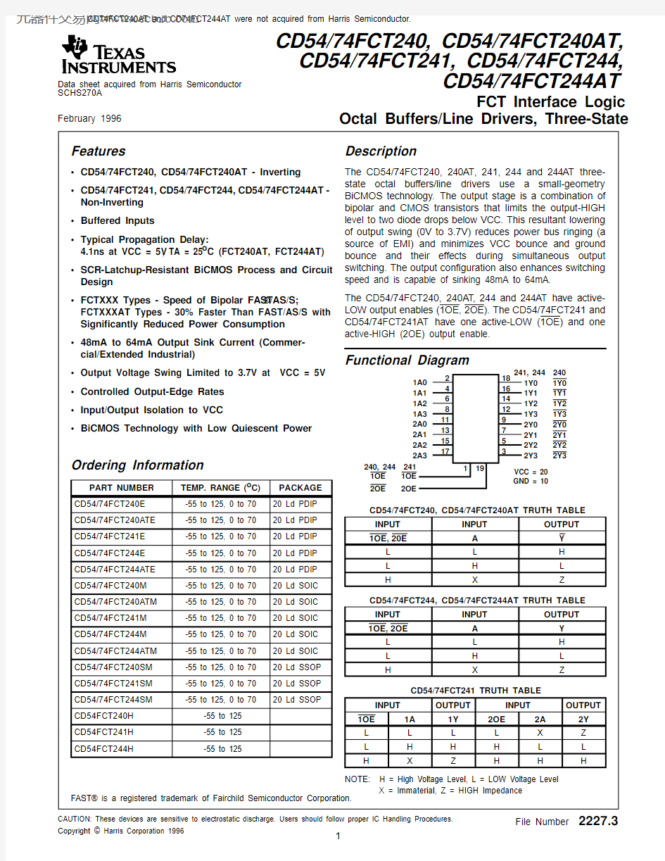
The CD54/74FCT240,240AT ,241,244and 244AT three-state octal buffers/line drivers use a small-geometry BiCMOS technology.The output stage is a combination of bipolar and CMOS transistors that limits the output-HIGH level to two diode drops below VCC.This resultant lowering of output swing (0V to 3.7V)reduces power bus ringing (a source of EMI)and minimizes VCC bounce and ground bounce and their effects during simultaneous output switching.The output con?guration also enhances switching speed and is capable of sinking 48mA to 64mA.
The CD54/74FCT240,240A T ,244and 244AT have active-LOW output enables (1OE,2OE).The CD54/74FCT241and CD54/74FCT241AT have one active-LOW (1OE)and one active-HIGH (2OE) output enable.
Functional Diagram
NOTE:
H = High Voltage Level, L = LOW Voltage Level X = Immaterial, Z = HIGH Impedance
Ordering Information
PART NUMBER TEMP. RANGE (o C)PACKAGE CD54/74FCT240E -55 to 125, 0 to 7020 Ld PDIP CD54/74FCT240ATE -55 to 125, 0 to 7020 Ld PDIP CD54/74FCT241E -55 to 125, 0 to 7020 Ld PDIP CD54/74FCT244E -55 to 125, 0 to 7020 Ld PDIP CD54/74FCT244ATE -55 to 125, 0 to 7020 Ld PDIP CD54/74FCT240M -55 to 125, 0 to 7020 Ld SOIC CD54/74FCT240ATM -55 to 125, 0 to 7020 Ld SOIC CD54/74FCT241M -55 to 125, 0 to 7020 Ld SOIC CD54/74FCT244M -55 to 125, 0 to 7020 Ld SOIC CD54/74FCT244ATM -55 to 125, 0 to 7020 Ld SOIC CD54/74FCT240SM -55 to 125, 0 to 7020 Ld SSOP CD54/74FCT241SM -55 to 125, 0 to 7020 Ld SSOP CD54/74FCT244SM -55 to 125, 0 to 70
20 Ld SSOP
CD54FCT240H -55 to 125CD54FCT241H -55 to 125CD54FCT244H
-55 to 125
CD54/74FCT240, CD54/74FCT240AT TRUTH TABLE INPUT INPUT OUTPUT
1OE,20E
A Y L L H L H L H
X
Z
CD54/74FCT244, CD54/74FCT244AT TRUTH TABLE INPUT INPUT OUTPUT
1OE,2OE
A Y L L H L H L H
X
Z
CD54/74FCT241 TRUTH TABLE
INPUT OUTPUT INPUT OUTPUT 1OE 1A 1Y 2OE
2A 2Y L L L L X Z L H H H L L H X
Z
H H
H
181614129753
2
46811131517
1
19
1A01A11A21A32A02A12A22A3
1OE 2OE
1Y01Y11Y21Y32Y02Y12Y22Y31Y01Y11Y21Y32Y02Y12Y22Y3
241, 2442401OE 2OE
240, 244241VCC = 20GND = 10
February 1996
CAUTION: These devices are sensitive to electrostatic discharge. Users should follow proper IC Handling Procedures.Copyright ? Harris Corporation 1996
File Number
2227.3
CD54/74FCT240, CD54/74FCT240AT,CD54/74FCT241, CD54/74FCT244,
CD54/74FCT244AT
FCT Interface Logic
Octal Buffers/Line Drivers, Three-State
FAST? is a registered trademark of Fairchild Semiconductor Corporation.
CD74FCT240AT and CD74FCT244AT were not acquired from Harris Semiconductor.元器件交易网https://www.wendangku.net/doc/6814486213.html,
Switching Speci?cations FCT Series tr, tf = 2.5ns, C L = 50pF, R L - See Figure 2
PARAMETER SYMBOL V CC
(V)
+25o
C
0o C to
+70o C
-55o C to
+125o C
+25o
C
0o C to
+70o C
-55o C to
+125o C
UNITS TYP MIN MAX MIN MAX TYP MIN MAX MIN MAX
Propagation Delays
Data to Outputs FCT240/AT t PLH,
t PHL
5?5 1.58 1.59 4.4 1.5 5.6 1.5 6.7ns
FCT241t PLH,
t PHL
54 1.5 6.5 1.57-----ns
FCT244/AT t PLH,
t PHL
5 4.5 1.5 6.5 1.57 3.8 1.5 5.3 1.5 6.2μs
Output Enable Times FCT240/AT t PZL,
t PZH
57 1.510 1.510.5 4.7 1.5 6.2 1.57.7μs
FCT241t PZL,
t PZH
5 5.5 1.58 1.58.5-----ns
FCT244/AT t PZL,
t PZH
56 1.58 1.58.5 4.8 1.5 6.5 1.57.8ns
Output Disable Times FCT240/AT t PLZ,
t PHZ
56 1.59.5 1.5104 1.5 5.6 1.5 6.5μs
FCT241t PLZ,
t PHZ
5 4.5 1.57 1.57.5-----ns
FCT244/AT t PLZ,
t PHZ
55 1.57 1.57.5 4.5 1.5 5.8 1.5 6.8μs
Power Dissipation
Capacitance
FCT240/AT C PD§-38 Typical38 Typical pF
FCT241 C PD§-33 Typical-pF
FCT244/AT C PD§35 Typical35 Typical pF
Min. (Valley) V OHV During Switch-ing of Other Outputs(Output Under Test Not Switching)
V OHV
See
Figure 1
50.5 Typical at +25o C V
Max. (Peak) V OLP During Switch-ing of Other Outputs(Output Under Test Not Switching)
V OLP
See
Figure 1
5 1 Typical at +25o C V
Input Capacitance C I---10-10--10-10pF 3-State Output Capacitance C O---15-15--15-15pF
?5V:min. is at 5.5V, max. is at 4.5V.
5V:min. is at 5.25V for 0o C to +70o C, max. is at 4.75V for 0o C to +70o C, typ. is at 5V
§C PD,measured per function,is used to determine the dynamic power consumption.P D(per package)=V CC I CC+∑(V CC2?C PD+V O2 fo C L + V CC?I CC D) where:
V CC = supply voltage
?I CC = flow through current x unit load
C L = output load capacitance
D = duty cycle of input high
fo = output frequency
fi = input frequency
CD54/74FCT540, CD54/74FCT540AT, CD54/74FCT241, CD54/74FCT244, CD54/74FCT244AT
2
IMPORTANT NOTICE
Texas Instruments and its subsidiaries (TI) reserve the right to make changes to their products or to discontinue any product or service without notice, and advise customers to obtain the latest version of relevant information to verify, before placing orders, that information being relied on is current and complete. All products are sold subject to the terms and conditions of sale supplied at the time of order acknowledgement, including those pertaining to warranty, patent infringement, and limitation of liability.
TI warrants performance of its semiconductor products to the specifications applicable at the time of sale in accordance with TI’s standard warranty. Testing and other quality control techniques are utilized to the extent TI deems necessary to support this warranty. Specific testing of all parameters of each device is not necessarily performed, except those mandated by government requirements.
CERTAIN APPLICATIONS USING SEMICONDUCTOR PRODUCTS MAY INVOLVE POTENTIAL RISKS OF DEATH, PERSONAL INJURY, OR SEVERE PROPERTY OR ENVIRONMENTAL DAMAGE (“CRITICAL APPLICATIONS”). TI SEMICONDUCTOR PRODUCTS ARE NOT DESIGNED, AUTHORIZED, OR WARRANTED TO BE SUITABLE FOR USE IN LIFE-SUPPORT DEVICES OR SYSTEMS OR OTHER CRITICAL APPLICATIONS. INCLUSION OF TI PRODUCTS IN SUCH APPLICATIONS IS UNDERSTOOD TO BE FULLY AT THE CUSTOMER’S RISK.
In order to minimize risks associated with the customer’s applications, adequate design and operating safeguards must be provided by the customer to minimize inherent or procedural hazards.
TI assumes no liability for applications assistance or customer product design. TI does not warrant or represent that any license, either express or implied, is granted under any patent right, copyright, mask work right, or other intellectual property right of TI covering or relating to any combination, machine, or process in which such semiconductor products or services might be or are used. TI’s publication of information regarding any third party’s products or services does not constitute TI’s approval, warranty or endorsement thereof.
Copyright ? 1999, Texas Instruments Incorporated