occ_pt
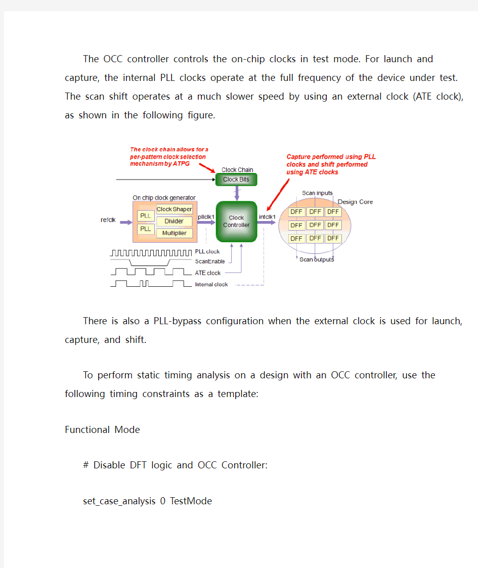

The OCC controller controls the on-chip clocks in test mode. For launch and capture, the internal PLL clocks operate at the full frequency of the device under test. The scan shift operates at a much slower speed by using an external clock (ATE clock), as shown in the following figure.
There is also a PLL-bypass configuration when the external clock is used for launch, capture, and shift.
To perform static timing analysis on a design with an OCC controller, use the following timing constraints as a template:
Functional Mode
# Disable DFT logic and OCC Controller:
set_case_analysis 0 TestMode
set_case_analysis 0 ScanEnable
Test Mode
# Enable DFT logic and OCC Controller:
set_case_analysis 1 TestMode
set_case_analysis 0 pll_bypass
set_case_analysis 0 pll_reset
# Set a false path constraint from the ScanEnable port (top-level)
# to the PLL clocks:
set_false_path -from ScanEnable -to { pllclk1 pllclk2 ... }
# Specify the asynchronous relationship between the PLL clocks (the PLL outputs)
# and the ATE clock:
set_clock_groups \
-name my_occ_clock_groups \
-asynchronous \
-group { ate_clk } \
-group { pllclk1 pllclk2 }
# If -common_launch_capture mode is used in TMAX (to avoid generating patterns # with one clock being used for launching the transition and another clock # being used for capturing the transition), apply the following timing
# constraints instead:
set_clock_groups \
-name my_occ_clock_groups \
-asynchronous \
-group { ate_clk } \
-group { pllclk1 } \
-group { pllclk2 }
# Set false paths from all ScanInput pins to the PLL clocks:
set_false_path -from test_si1 -to pllclk1
set_false_path -from test_si2 -to pllclk1
set_false_path -from ...
# Set multicycle paths with setup value of 3 and hold value of 2 from the # clock chain bits. The specific setup value of 3 applies to the DFTC-inserted # OCC controller. There are three delay elements (pipeline registers) to # synchronize the clock controller in order to prevent metastability. For # other OCC controllers, the path will be multi-cycle but the design should # be inspected to determine the actual number to be used.
set_multicycle_path -setup 3 -from
/top/snps_clk_chain_0/U_shftreg_0/ff_0/q_reg
set_multicycle_path -setup 3 -from
/top/snps_clk_chain_0/U_shftreg_0/ff_1/q_reg
set_multicycle_path -hold 2 -from
/top/snps_clk_chain_0/U_shftreg_0/ff_0/q_reg
set_multicycle_path -hold 2 -from
/top/snps_clk_chain_0/U_shftreg_0/ff_1/q_reg
# Apply a manual clock gating check to check the timing between the
# fast-clock-enable registers and the FastClock gates (multiplexers
# between the fast clocks and the slow clocks). PrimeTime does not
# perform clock gating checks on multiplexers by default.
set_clock_gating_check -high /top/snps_OCC_controller/U2
Note:
Do not run separate case analyses with ScanEnable 1 and ScanEnable 0. To make the clock gating check active in PrimeTime, the ScanEnable should be left without any case analysis.
OCC Bypass Mode
# Enable DFT logic and put OCC Controller in bypass mode:
set_case_analysis 1 TestMode
set_case_analysis 1 pll_bypass
set_case_analysis 0 pll_reset
Notes
This article uses the following terms:
?PLL clocks – The free-running clock outputs from the on-chip clock generator. They are used for the launch and capture of internal scanable elements that become internal clocks.
?ATE clock – The clock that shifts the scan chains according to the testing specifications.
?ScanEnable – The signal that enables switching between the ATE shift clock and output PLL clock signals. This signal is the same signal that drives the flip-flop's scan enable.
?TestMode –The top-level test_mode signal that is connected to the clock controller logic.
?pll_reset – The OCC reset that is used once during test setup and initialization.
?pll_bypass –The bypass signal that allows connection of the ATE clock signal directly to the internal clock signals, thus bypassing the PLL clocks.
?Clock chain – The scan chain segment of one or more scan cells. This chain allows for a per-pattern clock selection mechanism by ATPG. Clock selection values are loaded into the clock chain as part of the regular scan load process.
Controlling Clock Pulses in an OCC
Question:
My design has multiple on-chip clocks (OCCs). Two OCCs share the same PLL
voltage-controlled oscillator (VCO) source. I need one of the OCCs to run at half frequency. I see two options:
1) Constrain the half-frequency OCC shift register to either not deliver clocks or to deliver clocks in non-consecutive cycles (for example, use a shiftreg of 0000101).
2) Constrain the OCC so it will not deliver clocks by setting the shift registers
to zero. Then run a second-pass ATPG with a new, slower VCO in which only the half-frequency OCC is allowed to toggle.
How can I implement this?
Answer:
Here is how you can implement both options:
Option 1:
---------
Add a special section to your Test Protocol File. In the ClockStructures section
that describes the OCC, specify the following:
ClockStructures ScanCompression_mode {
PLLStructures "DFTC__pll_controller1" {
PLLCycles 4;
Clocks {
"ate_clk1" Reference;
"ref_clk" Reference;
"pllbuf1/Z" PLL {
OffState 0;
}
"DFTC__pll_controller1/DFTC_2/Z" Internal {
OffState 0;
PLLSource "pllbuf1/Z";
Cycle 0 "DFTC__snps_clk_chain_0/U_shftreg_0/ff_3/q_reg/Q" 1;
Cycle 1 "DFTC__snps_clk_chain_0/U_shftreg_0/ff_2/q_reg/Q" 1;
Cycle 2 "DFTC__snps_clk_chain_0/U_shftreg_0/ff_1/q_reg/Q" 1;
Cycle 3 "DFTC__snps_clk_chain_0/U_shftreg_0/ff_0/q_reg/Q" 1;
}
}
}
PLLStructures "DFTC__pll_controller2" {
PLLCycles 4;
Clocks {
"ate_clk1" Reference;
"ref_clk" Reference;
"pllbuf2/Z" PLL {
OffState 0;
}
"DFTC__pll_controller2/DFTC_2/Z" Internal {
OffState 0;
PLLSource "pllbuf2/Z";
Cycle 0 "DFTC__snps_clk_chain_1/U_shftreg_0/ff_3/q_reg/Q" 1;
Cycle 1 "DFTC__snps_clk_chain_1/U_shftreg_0/ff_2/q_reg/Q" 1;
Cycle 2 "DFTC__snps_clk_chain_1/U_shftreg_0/ff_1/q_reg/Q" 1;
Cycle 3 "DFTC__snps_clk_chain_1/U_shftreg_0/ff_0/q_reg/Q" 1;
}
}
}
ClockTiming CTiming_1 {
// This first group shows that the two clocks are not synchronized to each other.
// Since this is the default, it isn't really needed.
SynchronizedClocks group0 {
Clock fastclock { Location "DFTC__pll_controller1/DFTC_2/Z"; Period '10ns'; }
}
// This group specifies that this clock should only pulse on alternate cycles. // The Period specification is required by the syntax, but is only used if multiple clocks
// are synchronized to each other.
SynchronizedClocks group1 {
Clock slowclock { Location " DFTC__pll_controller2/DFTC_2/Z "; Period '10ns'; }
MultiCyclePath 2 { From "DFTC__pll_controller2/DFTC_2/Z"; To "DFTC__pll_controller2/DFTC_2/Z"; }
}
}
}
Note: You must use set_drc -multiframe_paths to enable this feature.
Option 2:
---------
If you want to constrain off the second OCC in the first ATPG run, you should set the following constraints and run DRC:
add_cell_constraints 0 DFTC__snps_clk_chain_1/U_shftreg_0/ff_1/q_reg
add_cell_constraints 0 DFTC__snps_clk_chain_1/U_shftreg_0/ff_0/q_reg
add_cell_constraints 0 DFTC__snps_clk_chain_1/U_shftreg_0/ff_2/q_reg
add_cell_constraints 0 DFTC__snps_clk_chain_1/U_shftreg_0/ff_3/q_reg
When the patterns are created, they will now only use the first internal clock source. A second run will be need to constrain off the first OCC and then allow the second one to be used.
How Can I Share the On-Chip Clocking Reset With the System Reset?
Question:
The current version of the Synopsys on-chip clocking (OCC) controller requires a reset signal. The OCC reset is used once during test_setup to initialize the OCC controller.
Can I share the OCC reset with the system reset?
Answer:
Yes, you can share the OCC and functional reset signals.
When doing the transition-delay test, the OCC reset must be pulsed once during the test_setup procedure and then held constant. During the transition-delay
test, you also need to keep the functional reset constant; otherwise, you will get timing violations. The functional reset is usually tested only in stuck-at mode, with OCC bypassed. There is no requirement to keep the OCC reset constant when the PLL is bypassed.
To share the OCC reset with the system reset, just define your reset signal as -type reset with -view existing_dft and also as -type pll_reset with
-view spec. For example:
set_dft_signal -view existing_dft -type reset -port rst -active_state 0
set_dft_signal -view spec -type pll_reset -port rst -active_state 0
DFT Compiler connects the reset to the OCC controller and writes the appropriate assignments into the test protocol file for the OCC and bypass modes.
Make sure that all shared reset specifications are using the same
-active_state statements. DFT Compiler accepts both active states 0 and 1 for the pll_reset and will automatically insert an inverter for the OCC
if necessary.