MAX4781ETE+中文资料

MAX4781/MAX4782/MAX4783
High-Speed, Low-Voltage, 0.7?CMOS Analog
Switches/Multiplexers
________________________________________________________________Maxim Integrated Products
1
19-2522; Rev 3; 2/05
For pricing delivery, and ordering information please contact Maxim/Dallas Direct!at
1-888-629-4642, or visit Maxim’s website at https://www.wendangku.net/doc/8a2926046.html,.
General Description
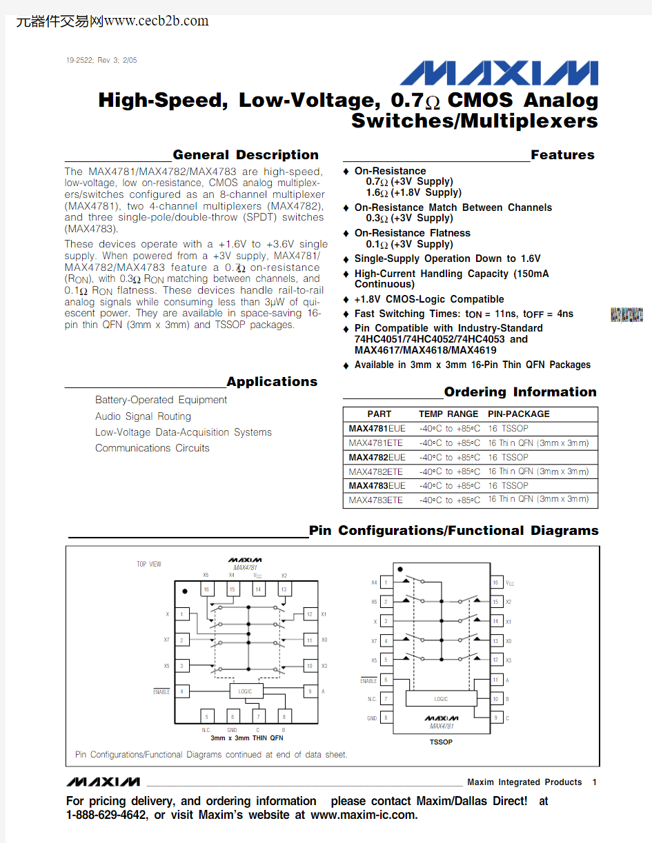
The MAX4781/MAX4782/MAX4783 are high-speed,low-voltage, low on-resistance, CMOS analog multiplex-ers/switches configured as an 8-channel multiplexer (MAX4781), two 4-channel multiplexers (MAX4782),and three single-pole/double-throw (SPDT) switches (MAX4783).
These devices operate with a +1.6V to +3.6V single supply. When powered from a +3V supply, MAX4781/MAX4782/MAX4783 feature a 0.7?on-resistance (R ON ), with 0.3?R ON matching between channels, and 0.1?R ON flatness. These devices handle rail-to-rail analog signals while consuming less than 3μW of qui-escent power. They are available in space-saving 16-pin thin QFN (3mm x 3mm) and TSSOP packages.
Applications
Battery-Operated Equipment Audio Signal Routing
Low-Voltage Data-Acquisition Systems Communications Circuits
Features
?On-Resistance
0.7?(+3V Supply)1.6?(+1.8V Supply)
?On-Resistance Match Between Channels
0.3?(+3V Supply)?On-Resistance Flatness
0.1?(+3V Supply)
?Single-Supply Operation Down to 1.6V ?High-Current Handling Capacity (150mA Continuous)
?+1.8V CMOS-Logic Compatible
?Fast Switching Times: t ON = 11ns, t OFF = 4ns ?Pin Compatible with Industry-Standard 74HC4051/74HC4052/74HC4053 and MAX4617/MAX4618/MAX4619
?Available in 3mm x 3mm 16-Pin Thin QFN Packages
Ordering Information
Pin Configurations/Functional Diagrams
M A X 4781/M A X 4782/M A X 4783
High-Speed, Low-Voltage, 0.7?CMOS Analog Switches/Multiplexers
ABSOLUTE MAXIMUM RATINGS
ELECTRICAL CHARACTERISTICS—Single +3V Supply
(V CC = +2.7V to +3.6V, GND = 0, V IH = 1.4V, V IL = 0.5V, T A = T MIN to T MAX , unless otherwise noted. Typical values are at T A = +25°C.) (Notes 2, 3)
Stresses beyond those listed under “Absolute Maximum Ratings” may cause permanent damage to the device. These are stress ratings only, and functional operation of the device at these or any other conditions beyond those indicated in the operational sections of the specifications is not implied. Exposure to absolute maximum rating conditions for extended periods may affect device reliability.
Voltages Referenced to GND
V CC , A, B, C, and ENABLE ...............................-0.3V to +4.6V Voltage at Any Other Terminal
(Note 1)...................................................-0.3V to (V CC + 0.3V)Continuous Current into A, B, C, ENABLE ........................±10mA Continuous Current into X, Y, Z, X_, Y_, Z_....................±150mA Peak Current into X, Y, Z, X_, Y_, Z_
(pulsed at 1ms, 10% duty cycle)................................±300mA
Continuous Power Dissipation
16-Pin Thin QFN (derate 16.9mW/°C above +70°C)...1349mW 16-Pin TSSOP (derate 5.7mW/°C above +70°C)........457mW Operating Temperature Range ..........................-40°C to +85°C Junction Temperature......................................................+150°C Storage Temperature Range.............................-65°C to +150°C Lead Temperature (soldering, 10s).................................+300°C
Note 1:Signals on X, Y, Z, X_, Y_, and Z_ exceeding V CC or GND are clamped by internal diodes. Limit forward-diode current to
maximum current rating.
MAX4781/MAX4782/MAX4783
High-Speed, Low-Voltage, 0.7?CMOS Analog
Switches/Multiplexers
_______________________________________________________________________________________3
ELECTRICAL CHARACTERISTICS—Single +3V Supply (continued)
(V CC = +2.7V to +3.6V, GND = 0, V IH = 1.4V, V IL = 0.5V, T A = T MIN to T MAX , unless otherwise noted. Typical values are at T A =+25°C.) (Notes 2, 3)
M A X 4781/M A X 4782/M A X 4783
High-Speed, Low-Voltage, 0.7?CMOS Analog Switches/Multiplexers 4_______________________________________________________________________________________
ELECTRICAL CHARACTERISTICS—Single +1.8V Supply
Note 4:R ON and ?R ON matching specifications for thin QFN-packaged parts are guaranteed by design.Note 5:?R ON = R ON(MAX)- R ON(MIN).
Note 6:Flatness is defined as the difference between the maximum and minimum value of on-resistance as measured over the
specified analog signal ranges.
Note 7:Guaranteed by design; not production tested.
Note 8:Off-isolation = 20log10(V COM_/ V NO ), V COM_= output, V NO = input to off switch.Note 9:Between any two channels.
MAX4781/MAX4782/MAX4783
High-Speed, Low-Voltage, 0.7?CMOS Analog
Switches/Multiplexers
_______________________________________________________________________________________5
ON-RESISTANCE vs. V X , V Y , V Z
V X , V Y , V Z (V)
R O N (?)
3.22.80.40.8 1.2 2.01.6 2.40.60.81.01.21.41.61.82.00.4
3.6
ON-RESISTANCE vs. V X , V Y , V Z ,
AND TEMPERATURE
V X , V Y , V Z (V)
R
O N (?)
2.5
0.5
1.0
1.5
2.0
0.10.2
0.30.40.60.50.70.90.81.000
3.0
1-40
85
60
10
35
-15
LEAKAGE CURRENT vs. TEMPERATURE
100
1000
10
TEMPERATURE (°C)
I X , I Y , I Z (p A )
CHARGE INJECTION vs. V X , V Y , V Z
V X , V Y , V Z (V)C H A R G E I N J E C T I O N (p C )
2.5
0.5
1.0
1.5
2.0
-100-80-60-20-400402060-120
3.0
10001.6
2.0
2.4
2.8
3.2 3.6
100
10
1
0.10.01
SUPPLY CURRENT vs. TEMPERATURE
V CC (V)
I C C (n A )
LOGIC THRESHOLD vs. SUPPLY VOLTAGE
SUPPLY VOLTAGE (V)
L O G I C T H R E S H O L D (V )
2.1
2.6
3.1
0.60.70.90.81.0
1.11.2
0.5
1.6
3.6
TURN-ON/TURN-OFF TIME vs. SUPPLY VOLTAGE
SUPPLY VOLTAGE (V)
T I M E (n s )
2.0
2.4
2.8
3.2
5
15
10
202501.6
3.6
TURN-ON/TURN-OFF TIME vs. TEMPERATURE
TEMPERATURE (°C)
T I M E (n s )
-15
10
35
60
286
410
1214
-40
85
Typical Operating Characteristics
(GND = 0, T A = +25°C, unless otherwise noted.)
M A X 4781/M A X 4782/M A X 4783
High-Speed, Low-Voltage, 0.7?CMOS Analog Switches/Multiplexers 6_______________________________________________________________________________________
Typical Operating Characteristics (continued)
(GND = 0, T A = +25°C, unless otherwise noted.)
MAX4781 Pin Description
FREQUENCY RESPONSE
FREQUENCY (Hz)
100
100k
1M
10M
1k
10k
100M
R E S P O N S E (d B )
-110
-90
-70-50
-3010-10
0.080.02
101k 10k
100
100k
TOTAL HARMONIC DISTORTION
vs. FREQUENCY
FREQUENCY (Hz)
T H D (%)
0.030.040.05
0.060.07
MAX4781/MAX4782/MAX4783
High-Speed, Low-Voltage, 0.7?CMOS Analog
Switches/Multiplexers
_______________________________________________________________________________________7
MAX4782 Pin Description
M A X 4781/M A X 4782/M A X 4783
High-Speed, Low-Voltage, 0.7?CMOS Analog Switches/Multiplexers 8_______________________________________________________________________________________
Applications Information
Power-Supply Considerations
Overview
The MAX4781/MAX4782/MAX4783 construction is typical of most CMOS analog switches. There are two supply inputs: V CC and GND. V CC and GND drive the internal CMOS switches and set the limits of the analog voltage on any switch. Internal reverse ESD-protection diodes are connected between each analog signal input and both V CC and GND. If any analog signal exceeds V CC or GND, one of these diodes conducts. During normal oper-ation, these and other reverse-biased ESD diodes leak,forming the only current drawn from V CC or GND.
Virtually all the analog leakage current comes from the ESD diodes. Although the ESD diodes on a given sig-nal input are identical and therefore fairly well bal-anced, they are reverse-biased differently. Each diode is biased by either V CC or GND and the analog signal.Their leakages vary as the signal varies. The difference in the two diodes’ leakages to V CC and GND consti-tutes the analog-signal-path leakage current. All analog leakage current flows between each input and one of the supply terminals, not to the other switch terminal.Both sides of a given switch can show leakage currents of either the same or opposite polarity.
V CC and GND power the internal logic and set the input logic limits. Logic inputs have ESD-protection diodes to ground.
Power Supply
The MAX4781/MAX4782/MAX4783 operate from a sin-gle supply between +1.6V and +3.6V. Switch on-resis-tance increases as the supply voltage is lowered.
High-Frequency Performance
In 50?systems, signal response is reasonably flat up to 50MH z (see the Typical Operating Characteristics ).Above 20MH z, the on-response has several minor peaks that are highly layout dependent. In the off state,the switch acts like a capacitor and passes higher fre-quencies with less attenuation. At 10MH z, off-isolation is approximately -50dB in 50?systems, becoming worse (approximately 20dB per decade) as frequency increases. Higher circuit impedance also degrades off-isolation. Adjacent channel attenuation is approximate-ly 3dB above that of a bare IC socket and is entirely because of capacitive coupling.
Pin Nomenclature
The MAX4781/MAX4782/MAX4783 are pin compatible with the industry-standard 74H C4051/74H C4052/74H C4053 and the MAX4617/MAX4618/MAX4619. In single-supply applications, they function identically and have identical logic diagrams, although these parts dif-fer electrically. The pin designations and logic dia-grams in this data sheet conform to the original 1972specifications published by RCA for the CD4051/CD4052/CD4053. These designations differ from the standard Maxim switch and mux designations found on other Maxim data sheets such as the MAX4051/MAX4052/MAX4053. Designers who are more comfort-able with Maxim’s standard designations are advised that the pin designations and logic diagrams on the MAX4051/MAX4052/MAX4053 data sheet can be applied to the MAX4781/MAX4782/MAX4783.
?= Don’t care.
*Not present on MAX4782.
Note:Input and output pins are identical and interchangeable. Either can be considered an input or output. Signals pass equally
well in either direction.
MAX4781/MAX4782/MAX4783
High-Speed, Low-Voltage, 0.7?CMOS Analog
Switches/Multiplexers
_______________________________________________________________________________________9
M A X 4781/M A X 4782/M A X 4783
High-Speed, Low-Voltage, 0.7?CMOS Analog Switches/Multiplexers 10______________________________________________________________________________________
Test Circuits/Timing Diagrams
Figure 1. Enable Switching Times
MAX4781/MAX4782/MAX4783
High-Speed, Low-Voltage, 0.7?CMOS Analog
Switches/Multiplexers
______________________________________________________________________________________11
Test Circuits/Timing Diagrams (continued)
Figure 2. Address Transition Times
M A X 4781/M A X 4782/M A X 4783
High-Speed, Low-Voltage, 0.7?CMOS Analog Switches/Multiplexers 12______________________________________________________________________________________
Test Circuits/Timing Diagrams (continued)
Figure 3. Break-Before-Make Interval
Figure 4. Charge Injection
MAX4781/MAX4782/MAX4783
High-Speed, Low-Voltage, 0.7?CMOS Analog
Switches/Multiplexers
______________________________________________________________________________________13
Test Circuits/Timing Diagrams (continued)
Figure 5. Off-Isolation, On-Loss, and Crosstalk
Figure 6. Capacitance
Chip Information
TRANSISTOR COUNT: 659PROCESS: CMOS
M A X 4781/M A X 4782/M A X 4783
High-Speed, Low-Voltage, 0.7?CMOS Analog Switches/Multiplexers
Pin Configurations/Functional Diagrams (continued)
MAX4781/MAX4782/MAX4783
High-Speed, Low-Voltage, 0.7?CMOS Analog
Switches/Multiplexers
______________________________________________________________________________________15
Package Information
(The package drawing(s) in this data sheet may not reflect the most current specifications. For the latest package outline information,go to https://www.wendangku.net/doc/8a2926046.html,/packages .)
M A X 4781/M A X 4782/M A X 4783
High-Speed, Low-Voltage, 0.7?CMOS Analog Switches/Multiplexers Maxim cannot assume responsibility for use of any circuitry other than circuitry entirely embodied in a Maxim product. No circuit patent licenses are implied. Maxim reserves the right to change the circuitry and specifications without notice at any time.
16____________________Maxim Integrated Products, 120 San Gabriel Drive, Sunnyvale, CA 94086 408-737-7600?2005 Maxim Integrated Products
Printed USA
is a registered trademark of Maxim Integrated Products, Inc.
Package Information (continued)
(The package drawing(s) in this data sheet may not reflect the most current specifications. For the latest package outline information,go to https://www.wendangku.net/doc/8a2926046.html,/packages .)