LM4808

LM4808
Dual 105mW Headphone Amplifier
General Description
The LM4808is a dual audio power amplifier capable of delivering 105mW per channel of continuous average power into a 16?load with 0.1%(THD+N)from a 5V power supply.Boomer audio power amplifiers were designed specifically to provide high quality output power with a minimal amount of external components using surface mount packaging.Since the LM4808does not require bootstrap capacitors or snub-ber networks,it is optimally suited for low-power portable systems.
The unity-gain stable LM4808can be configured by external gain-setting resistors.
Key Specifications
n THD+N at 1kHz at 105mW continuous average output power into 16?0.1%(typ)n THD+N at 1kHz at 70mW continuous average output power into 32?0.1%(typ)n Output power at 0.1%THD+N at 1kHz into 32?70mW (typ)
Features
n LLP ,MSOP ,and SOP surface mount packaging n Switch on/off click suppression
n Excellent power supply ripple rejection n Unity-gain stable
n
Minimum external components
Applications
n Headphone Amplifier n Personal Computers
n Portable electronic devices
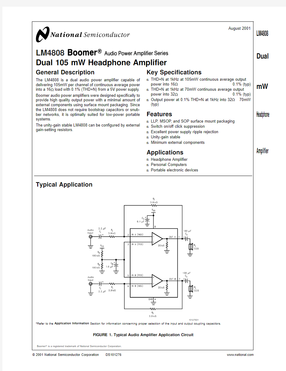
Typical Application
Boomer ?is a registered trademark of National Semiconductor Corporation.
10127601
*Refer to the Application Information Section for information concerning proper selection of the input and output coupling capacitors.
FIGURE 1.Typical Audio Amplifier Application Circuit
August 2001
LM4808Dual 105mW Headphone Amplifier
?2001National Semiconductor Corporation https://www.wendangku.net/doc/853164854.html,
Connection Diagrams
LLP Package
10127657
Top View
Order Number LM4808LD
See NS Package Number LDA08B
SOP &MSOP Package
10127602
Top View
Order Number LM4808M,LM4808MM See NS Package Number M08A,MUA08A
L M 4808
https://www.wendangku.net/doc/853164854.html, 2
Absolute Maximum Ratings
(Note 3)
If Military/Aerospace specified devices are required,please contact the National Semiconductor Sales Office/Distributors for availability and specifications.Supply Voltage 6.0V
Storage Temperature ?65?C to +150?C Input Voltage
?0.3V to V DD +0.3V
Power Dissipation (Note 4)Internally limited
ESD Susceptibility (Note 5)3500V ESD Susceptibility (Note 6)250V Junction Temperature 150?C
Soldering Information (Note 1)Small Outline Package Vapor Phase (60seconds)215?C Infrared (15seconds)220?C Thermal Resistance
θJC (MSOP)56?C/W θJA (MSOP)210?C/W θJC (SOP)35?C/W θJA (SOP)170?C/W θJC (LLP)15?C/W
θJA (LLP)117?C/W (Note 9)θJA (LLP)
150?C/W (Note 10)
Operating Ratings
Temperature Range T MIN ≤T A ≤T MAX ?40?C ≤T
A
≤85?C
Supply Voltage
2.0V ≤V DD ≤5.5V
Note 1:See AN-450“Surface Mounting and their Effects on Product Reli-ability”for other methods of soldering surface mount devices.
Electrical Characteristics (Notes 2,3)
The following specifications apply for V DD =5V unless otherwise specified,limits apply to T A =25?C.Symbol
Parameter
Conditions
LM4808
Units (Limits)Typ (Note 7)Limit (Note
8)
V DD Supply Voltage 2.0V (min)5.5
V (max)I DD Supply Current V IN =0V,I O =0A 1.2 3.0mA (max)P tot Total Power Dissipation V IN =0V,I O =0A 616.5mW (max)V OS Input Offset Voltage V IN =0V
1050
mV (max)
Ibias Input Bias Current 10pA V CM Common Mode Voltage 0V 4.3
V G V Open-Loop Voltage Gain R L =5k ?67dB Io Max Output Current THD+N <0.1%
70mA R O Output Resistance 0.1?V O Output Swing
R L =32?,0.1%THD+N,Min .3V R L =32?,0.1%THD+N,Max 4.7PSRR Power Supply Rejection Ratio Cb =1.0μF,Vripple =100mV PP ,
f =100Hz 89dB Crosstalk Channel Separation
R L =32?75dB THD+N
Total Harmonic Distortion +Noise
f =1kHz
R L =16?,
V O =3.5V PP (at 0dB)0.05%66dB R L =32?,
V O =3.5V PP (at 0dB)
0.05%66dB SNR Signal-to-Noise Ratio V O =3.5V pp (at 0dB)105dB f G Unity Gain Frequency Open Loop,R L =5k ? 5.5MHz P o
Output Power
THD+N =0.1%,f =1kHz R L =16?105mW
R L =32?
7060mW THD+N =10%,f =1kHz R L =16?150mW R L =32?
90mW C I
Input Capacitance
3
pF
LM4808
https://www.wendangku.net/doc/853164854.html,
3
Electrical Characteristics (Notes 2,3)
(Continued)
The following specifications apply for V DD
=5V unless otherwise specified,limits apply to T A =25?C.
Symbol
Parameter
Conditions
LM4808
Units
(Limits)Typ (Note 7)Limit (Note
8)
C L Load Capacitance 200
pF SR
Slew Rate
Unity Gain Inverting
3
V/μs
Electrical Characteristics (Notes 2,3)
The following specifications apply for V DD =3.3V unless otherwise specified,limits apply to T A =25?C.Symbol
Parameter
Conditions
Conditions Units
(Limits)Typ (Note 7)Limit (Note
8)
I DD Supply Current V IN =0V,I O =0A 1.0mA (max)V OS Input Offset Voltage V IN =0V
7
mV (max)
P o
Output Power
THD+N =0.1%,f =1kHz R L =16?40mW R L =32?
28
mW
THD+N =10%,f =1kHz R L =16?56mW R L =32?
38
mW
Electrical Characteristics (Notes 2,3)
The following specifications apply for V DD =2.6V unless otherwise specified,limits apply to T A =25?C.Symbol
Parameter
Conditions
Conditions Units (Limits)Typ (Note 7)Limit (Note
8)
I DD Supply Current V IN =0V,I O =0A 0.9mA (max)V OS Input Offset Voltage V IN =0V
5mV (max)P o
Output Power
THD+N =0.1%,f =1kHz R L =16?20mW R L =32?
16mW THD+N =10%,f =1kHz R L =16?31mW R L =32?
22
mW
Note 2:All voltages are measured with respect to the ground pin,unless otherwise specified.
Note 3:Absolute Maximum Ratings indicate limits beyond which damage to the device may occur.Operating Ratings indicate conditions for which the device is
functional,but do not guarantee specific performance limits.Electrical Characteristics state DC and AC electrical specifications under particular test conditions which guarantee specific performance limits.This assumes that the device is within the Operating Ratings.Specifications are not guaranteed for parameters where no limit is given,however,the typical value is a good indication of device performance.
Note 4:The maximum power dissipation must be derated at elevated temperatures and is dictated by T JMAX ,θJA ,and the ambient temperature T A .The maximum allowable power dissipation is P DMAX =(T JMAX ?T A )/θJA .For the LM4808,T JMAX =150?C,and the typical junction-to-ambient thermal resistance,when board mounted,is 210?C/W for package MUA08A and 170?C/W for package M08A.Note 5:Human body model,100pF discharged through a 1.5k ?resistor.Note 6:Machine Model,220pF–240pF discharged through all pins.Note 7:Typicals are measured at 25?C and represent the parametric norm.
Note 8:Tested limits are guaranteed to National’s AOQL (Average Outgoing Quality Level).Datasheet min/max specification limits are guaranteed by design,test,or statistical analysis.
Note 9:The given θJA is for an LM4808packaged in an LDA08B with the Exposed-DAP soldered to a printed circuit board copper pad with an area equivalent to that of the Exposed-DAP itself.
Note 10:The given θJA is for an LM4808packaged in an LDA08B with the Exposed-DAP not soldered to any printed circuit board copper.
L M 4808
https://www.wendangku.net/doc/853164854.html, 4
External Components Description
(Figure 1)
Components Functional Description
1.R i
The inverting input resistance,along with R f ,set the closed-loop gain.R i ,along with C i ,form a high pass filter with f c =1/(2πR i C i ).
2.C i The input coupling capacitor blocks DC voltage at the amplifier’s input terminals.C i ,along with R i ,create a highpass filter with f C =1/(2πR i C i ).Refer to the section,Selecting Proper External Components ,for an explanation of determining the value of C i .
3.R f The feedback resistance,along with R i ,set closed-loop gain.
4.C S
This is the supply bypass capacitor.It provides power supply filtering.Refer to the Application Information section for proper placement and selection of the supply bypass capacitor.
5.C B
This is the half-supply bypass pin capacitor.It provides half-supply filtering.Refer to the section,
Selecting Proper External Components ,for information concerning proper placement and selection of C B .
6.C O This is the output coupling capacitor.It blocks the DC voltage at the amplifier’s output and forms a high pass filter with R L at f O =1/(2πR L C O )
7.R B
This is the resistor which forms a voltage divider that provides 1/2V DD to the non-inverting input of the amplifier.
Typical Performance Characteristics
THD+N vs Frequency
THD+N vs Frequency
1012760310127604
THD+N vs Frequency THD+N vs Frequency
1012760510127606
LM4808
https://www.wendangku.net/doc/853164854.html,
5
Typical Performance Characteristics
(Continued)
THD+N vs Frequency
THD+N vs Frequency
1012760710127608
THD+N vs Frequency THD+N vs Frequency
1012760910127610
THD+N vs Frequency THD+N vs Frequency
1012761110127612
L M 4808
https://www.wendangku.net/doc/853164854.html, 6
Typical Performance Characteristics
(Continued)
THD+N vs Output Power
THD+N vs Output Power
1012761310127614
THD+N vs Output Power THD+N vs Output Power
1012761510127616
THD+N vs Output Power THD+N vs Output Power
1012761710127618
LM4808
https://www.wendangku.net/doc/853164854.html,
7
Typical Performance Characteristics
(Continued)
THD+N vs Output Power
THD+N vs Output Power
1012761910127620
THD+N vs Output Power
Output Power vs Load Resistance
10127621
10127622
Output Power vs Load Resistance Output Power vs Load Resistance
1012762310127624
L M 4808
https://www.wendangku.net/doc/853164854.html, 8
Typical Performance Characteristics(Continued)
Output Power vs Supply Voltage
Output Power vs
Power Supply 1012762510127626
Output Power vs Power Supply
Clipping Voltage vs
Supply Voltage 1012762710127628
Power Dissipation vs Output Power
Power Dissipation vs
Output Power
1012762910127630
LM4808
https://www.wendangku.net/doc/853164854.html,
9
Typical Performance Characteristics
(Continued)
Power Dissipation vs
Output Power
Channel Separation
10127631
10127632
Channel Separation Noise Floor
10127633
10127634
Power Supply Rejection Ratio
Open Loop
Frequency Response
10127635
10127650
L M 4808
https://www.wendangku.net/doc/853164854.html, 10
Typical Performance Characteristics
(Continued)
Open Loop
Frequency Response
Open Loop
Frequency Response
1012765110127638
Supply Current vs Supply Voltage Frequency Response vs Output Capacitor Size
10127644
10127645
Frequency Response vs Output Capacitor Size Frequency Response vs Output Capacitor Size
1012764610127647
LM4808
https://www.wendangku.net/doc/853164854.html,
11
Typical Performance Characteristics
(Continued)
Typical Application Frequency Response
Typical Application Frequency Response
1012764810127649
L M 4808
https://www.wendangku.net/doc/853164854.html, 12
Application Information
EXPOSED-DAP PACKAGE PCB MOUNTING CONSIDERATION
The LM4808’s exposed-dap(die attach paddle)package (LD)provides a low thermal resistance between the die and the PCB to which the part is mounted and soldered.This allows rapid heat transfer from the die to the surrounding PCB copper traces,ground plane,and surrounding air. The LD package should have its DAP soldered to a copper pad on the PCB.The DAP’s PCB copper pad may be con-nected to a large plane of continuous unbroken copper.This plane forms a thermal mass,heat sink,and radiation area. However,since the LM4808is designed for headphone ap-plications,connecting a copper plane to the DAP’s PCB copper pad is not required.The LM4808’s Power Dissipation vs Output Power Curve in the Typical Performance Char-acteristics shows that the maximum power dissipated is just 45mW per amplifier with a5V power supply and a32?load. Further detailed and specific information concerning PCB layout,fabrication,and mounting an LD(LLP)package is available from National Semiconductor’s Package Engineer-ing Group under application note AN1187.
POWER DISSIPATION
Power dissipation is a major concern when using any power amplifier and must be thoroughly understood to ensure a successful design.Equation1states the maximum power dissipation point for a single-ended amplifier operating at a given supply voltage and driving a specified output load.
P DMAX=(V DD)2/(2π2R L)(1)
Since the LM4808has two operational amplifiers in one package,the maximum internal power dissipation point is twice that of the number which results from Equation1.Even with the large internal power dissipation,the LM4808does not require heat sinking over a large range of ambient tem-perature.From Equation1,assuming a5V power supply and a32?load,the maximum power dissipation point is40mW per amplifier.Thus the maximum package dissipation point is80mW.The maximum power dissipation point obtained must not be greater than the power dissipation that results from Equation2:
P DMAX=(T JMAX?T A)/θJA(2)
For package MUA08A,θJA=210?C/W.T JMAX=150?C for the LM4808.Depending on the ambient temperature,T A,of the system surroundings,Equation2can be used to find the maximum internal power dissipation supported by the IC packaging.If the result of Equation1is greater than that of Equation2,then either the supply voltage must be de-creased,the load impedance increased or T A reduced.For the typical application of a5V power supply,with a32?load, the maximum ambient temperature possible without violating the maximum junction temperature is approximately133.2?C provided that device operation is around the maximum power dissipation point.Power dissipation is a function of output power and thus,if typical operation is not around the maximum power dissipation point,the ambient temperature may be increased accordingly.Refer to the Typical Perfor-mance Characteristics curves for power dissipation infor-mation for lower output powers.
POWER SUPPLY BYPASSING
As with any power amplifier,proper supply bypassing is
critical for low noise performance and high power supply
rejection.Applications that employ a5V regulator typically
use a10μF in parallel with a0.1μF filter capacitors to stabi-
lize the regulator’s output,reduce noise on the supply line,
and improve the supply’s transient response.However,their
presence does not eliminate the need for a local0.1μF
supply bypass capacitor,C S,connected between the
LM4808’s supply pins and ground.Keep the length of leads
and traces that connect capacitors between the LM4808’s
power supply pin and ground as short as possible.Connect-
ing a1.0μF capacitor,C B,between the IN A(+)/IN B(+)node
and ground improves the internal bias voltage’s stability and
improves the amplifier’s PSRR.The PSRR improvements
increase as the bypass pin capacitor value increases.Too
large,however,increases the amplifier’s turn-on time.The
selection of bypass capacitor values,especially C B,depends
on desired PSRR requirements,click and pop performance
(as explained in the section,Selecting Proper External
Components),system cost,and size constraints.
SELECTING PROPER EXTERNAL COMPONENTS
Optimizing the LM4808’s performance requires properly se-
lecting external components.Though the LM4808operates
well when using external components with wide tolerances,
best performance is achieved by optimizing component val-
ues.
The LM4808is unity-gain stable,giving a designer maximum
design flexibility.The gain should be set to no more than a
given application requires.This allows the amplifier to
achieve minimum THD+N and maximum signal-to-noise ra-
tio.These parameters are compromised as the closed-loop
gain increases.However,low gain demands input signals
with greater voltage swings to achieve maximum output
power.Fortunately,many signal sources such as audio
CODECs have outputs of1V RMS(2.83V P-P).Please refer to
the Audio Power Amplifier Design section for more infor-
mation on selecting the proper gain.
Input and Output Capacitor Value Selection
Amplifying the lowest audio frequencies requires high value
input and output coupling capacitors(C I and C O in Figure1).
A high value capacitor can be expensive and may compro-
mise space efficiency in portable designs.In many cases,
however,the speakers used in portable systems,whether
internal or external,have little ability to reproduce signals
below150Hz.Applications using speakers with this limited
frequency response reap little improvement by using high
value input and output capacitors.
Besides affecting system cost and size,C i has an effect on
the LM4808’s click and pop performance.The magnitude of
the pop is directly proportional to the input capacitor’s size.
Thus,pops can be minimized by selecting an input capacitor
value that is no higher than necessary to meet the desired
?3dB frequency.
As shown in Figure1,the input resistor,R I and the input
capacitor,C I,produce a?3dB high pass filter cutoff fre-
quency that is found using Equation(3).In addition,the
output load R L,and the output capacitor C O,produce a-3db
high pass filter cutoff frequency defined by Equation(4).
f I-3db=1/2πR I C I(3)
f O-3db=1/2πR L C O(4)
LM4808
https://www.wendangku.net/doc/853164854.html,
13
Application Information(Continued)
Also,careful consideration must be taken in selecting a
certain type of capacitor to be used in the system.Different
types of capacitors(tantalum,electrolytic,ceramic)have
unique performance characteristics and may affect overall
system performance.
Bypass Capacitor Value
Besides minimizing the input capacitor size,careful consid-
eration should be paid to the value of the bypass capacitor,
C B.Since C B determines how fast the LM4808settles to
quiescent operation,its value is critical when minimizing
turn-on pops.The slower the LM4808’s outputs ramp to their
quiescent DC voltage(nominally1/2V DD),the smaller the
turn-on pop.Choosing C B equal to 1.0μF or larger,will
minimize turn-on pops.As discussed above,choosing C i no
larger than necessary for the desired bandwith helps mini-
mize clicks and pops.
AUDIO POWER AMPLIFIER DESIGN
Design a Dual70mW/32?Audio Amplifier
Given:
Power Output70mW
Load Impedance32?
Input Level1Vrms(max)
Input Impedance20k?
Bandwidth100Hz–20kHz±0.50dB
The design begins by specifying the minimum supply voltage
necessary to obtain the specified output power.One way to
find the minimum supply voltage is to use the Output Power
vs Supply Voltage curve in the Typical Performance Char-
acteristics section.Another way,using Equation(5),is to
calculate the peak output voltage necessary to achieve the
desired output power for a given load impedance.To ac-
count for the amplifier’s dropout voltage,two additional volt-
ages,based on the Dropout Voltage vs Supply Voltage in the
Typical Performance Characteristics curves,must be
added to the result obtained by Equation(5).For a
single-ended application,the result is Equation(6).
(5)
V DD≥(2V OPEAK+(V OD
TOP
+V OD
BOT
))(6)
The Output Power vs Supply Voltage graph for a32?load
indicates a minimum supply voltage of4.8V.This is easily
met by the commonly used5V supply voltage.The additional
voltage creates the benefit of headroom,allowing the
LM4808to produce peak output power in excess of70mW
without clipping or other audible distortion.The choice of
supply voltage must also not create a situation that violates
maximum power dissipation as explained above in the
Power Dissipation section.Remember that the maximum
power dissipation point from Equation(1)must be multiplied
by two since there are two independent amplifiers inside the
package.Once the power dissipation equations have been
addressed,the required gain can be determined from Equa-
tion(7).
(7)
Thus,a minimum gain of1.497allows the LM4808to reach
full output swing and maintain low noise and THD+N perfro-
mance.For this example,let A V=1.5.
The amplifiers overall gain is set using the input(R i)and
feedback(R f)resistors.With the desired input impedance
set at20k?,the feedback resistor is found using Equation
(8).
A V=R f/R i(8)
The value of R f is30k?.
The last step in this design is setting the amplifier’s?3db
frequency bandwidth.To achieve the desired±0.25dB pass
band magnitude variation limit,the low frequency response
must extend to at lease one?fifth the lower bandwidth limit
and the high frequency response must extend to at least five
times the upper bandwidth limit.The gain variation for both
response limits is0.17dB,well within the±0.25dB desired
limit.The results are an
f L=100Hz/5=20Hz(9)
and a
f H=20kHz*5=100kHz(10)
As stated in the External Components section,both R i in
conjunction with C i,and C o with R L,create first order high-
pass filters.Thus to obtain the desired low frequency re-
sponse of100Hz within±0.5dB,both poles must be taken
into consideration.The combination of two single order filters
at the same frequency forms a second order response.This
results in a signal which is down0.34dB at five times away
from the single order filter?3dB point.Thus,a frequency of
20Hz is used in the following equations to ensure that the
response is better than0.5dB down at100Hz.
C i≥1/(2π*20k?*20Hz)=0.397μF;use0.39μF.
C o≥1/(2π*32?*20Hz)=249μF;use330μF.
The high frequency pole is determined by the product of the
desired high frequency pole,f H,and the closed-loop gain,
A V.With a closed-loop gain of1.5and f H=100kHz,the
resulting GBWP=150kHz which is much smaller than the
LM4808’s GBWP of900kHz.This figure displays that if a
designer has a need to design an amplifier with a higher
gain,the LM4808can still be used without running into
bandwidth limitations.
L
M
4
8
8
https://www.wendangku.net/doc/853164854.html,14
Demonstration Board Layout
10127639
Recommended SO PC Board Layout:
Top Silkscreen
10127660
Recommended LD PC Board Layout:
Top Silkscreen
10127640
Recommended SOP PC Board Layout:
Top Layer
10127661
Recommended LD PC Board Layout:
Top Layer
10127642
Recommended SOP PC Board Layout:
Bottom Layer
10127662
Recommended LD PC Board Layout:
Bottom Layer
LM4808
https://www.wendangku.net/doc/853164854.html,
15
Physical Dimensions
inches (millimeters)
unless otherwise noted
Order Number LM4808LD NS Package Number LDA08B
Order Number LM4808M NS Package Number M08A
L M 4808
https://www.wendangku.net/doc/853164854.html, 16
Physical Dimensions
inches (millimeters)unless otherwise noted (Continued)
Order Number LM4808MM NS Package Number MUA08A
LIFE SUPPORT POLICY
NATIONAL’S PRODUCTS ARE NOT AUTHORIZED FOR USE AS CRITICAL COMPONENTS IN LIFE SUPPORT DEVICES OR SYSTEMS WITHOUT THE EXPRESS WRITTEN APPROVAL OF THE PRESIDENT AND GENERAL COUNSEL OF NATIONAL SEMICONDUCTOR CORPORATION.As used herein:1.Life support devices or systems are devices or systems which,(a)are intended for surgical implant into the body,or (b)support or sustain life,and whose failure to perform when properly used in accordance with instructions for use provided in the labeling,can be reasonably expected to result in a significant injury to the user.
2.A critical component is any component of a life support device or system whose failure to perform can be reasonably expected to cause the failure of the life support device or system,or to affect its safety or effectiveness.
National Semiconductor Corporation Americas
Email:support@https://www.wendangku.net/doc/853164854.html,
National Semiconductor Europe
Fax:+49(0)180-5308586Email:europe.support@https://www.wendangku.net/doc/853164854.html,
Deutsch Tel:+49(0)6995086208English Tel:+44(0)8702402171Fran?ais Tel:+33(0)141918790
National Semiconductor Asia Pacific Customer Response Group Tel:65-2544466Fax:65-2504466
Email:ap.support@https://www.wendangku.net/doc/853164854.html,
National Semiconductor Japan Ltd.
Tel:81-3-5639-7560Fax:81-3-5639-7507
https://www.wendangku.net/doc/853164854.html,
LM4808Dual 105mW Headphone Amplifier
National does not assume any responsibility for use of any circuitry described,no circuit patent licenses are implied and National reserves the right at any time without notice to change said circuitry and specifications.