A Switchable Digital–Analog Low-Dropout Regulator for Analog Dynamic Voltage Scaling Technique
A Switchable Digital–Analog Low-Dropout
Regulator for Analog Dynamic
V oltage Scaling Technique
Wei-Chung Chen,Student Member,IEEE,Su-Yi Ping,Tzu-Chi Huang,Yu-Huei Lee,Student Member,IEEE, Ke-Horng Chen,Senior Member,IEEE,and Chin-Long Wey,Fellow,IEEE
Abstract—Dual dynamic voltage scaling(DVS)techniques em-ployed in single-inductor dual-output(SIDO)converters are used to improve the ef?ciency of the system-on-a-chip(SoC).One DVS technique for digital circuits is controlled by the SoC processor. This paper presents the analog DVS(ADVS)technique for analog circuits to scale voltage across the power MOSFET of the switch-able digital–analog(D/A)low-dropout(LDO)regulator which is the post-regulator cascaded in series with the SIDO converter.The ADVS determines the tradeoff between voltage suppression and ef-?ciency.Furthermore,because of the digital operation of the D/A LDO regulator,the quiescent current is further reduced at light loads while the load current requirement is minimized.In addi-tion,the limitation of the capacitor-free LDO is signi?cantly re-duced by a few microamperes.The test chip was fabricated using a 40-nm CMOS process.Experimental results demonstrated switch-able D/A LDO regulator operation with peak ef?ciency at96.7%in analog operation and a5-mV output voltage ripple at120-mA load resulting from the advantage of ripple suppression.The power ef-?ciency could be sustained at a value over92.57%even when the load current decreased to1 A.
Index Terms—Asynchronous digital low-dropout(LDO)regu-lator,bidirectional asynchronous signal pipeline,dynamic voltage scaling(DVS),hybrid operation,million instructions per second performance,power conversion ef?ciency,power module,ripple-based control,switching regulator.
I.I NTRODUCTION
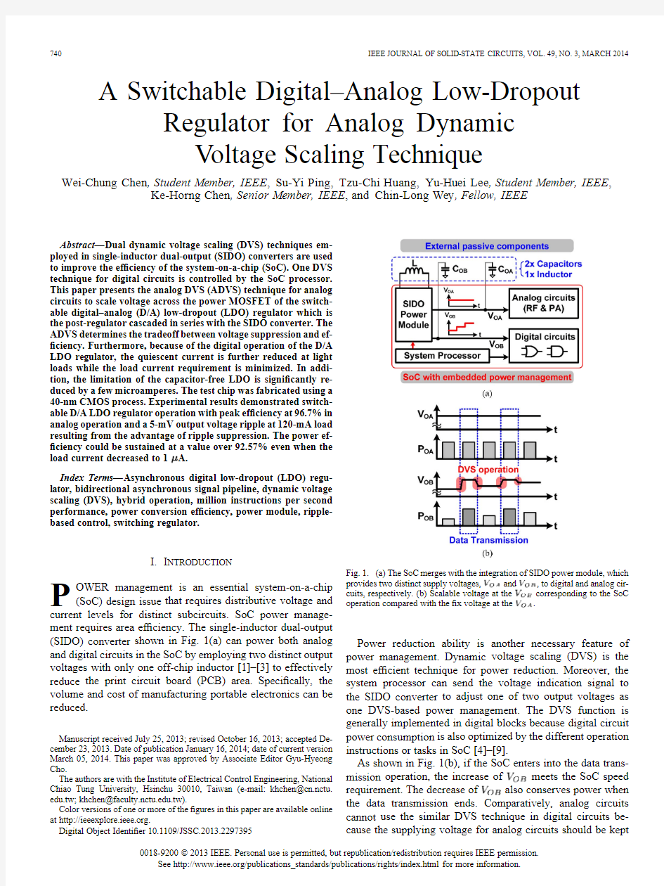
P OWER management is an essential system-on-a-chip (SoC)design issue that requires distributive voltage and current levels for distinct subcircuits.SoC power manage-ment requires area ef?ciency.The single-inductor dual-output (SIDO)converter shown in Fig.1(a)can power both analog and digital circuits in the SoC by employing two distinct output voltages with only one off-chip inductor[1]–[3]to effectively reduce the print circuit board(PCB)area.Speci?cally,the volume and cost of manufacturing portable electronics can be reduced.
Manuscript received July25,2013;revised October16,2013;accepted De-cember23,2013.Date of publication January16,2014;date of current version March05,2014.This paper was approved by Associate Editor Gyu-Hyeong Cho.
The authors are with the Institute of Electrical Control Engineering,National Chiao Tung University,Hsinchu30010,Taiwan(e-mail:khchen@cn.nctu. edu.tw;khchen@https://www.wendangku.net/doc/8f13056105.html,.tw).
Color versions of one or more of the?gures in this paper are available online at https://www.wendangku.net/doc/8f13056105.html,.
Digital Object Identi?er
10.1109/JSSC.2013.2297395Fig.1.(a)The SoC merges with the integration of SIDO power module,which provides two distinct supply voltages,and,to digital and analog cir-cuits,respectively.(b)Scalable voltage at the corresponding to the SoC operation compared with the?x voltage at the.
Power reduction ability is another necessary feature of power management.Dynamic voltage scaling(DVS)is the most ef?cient technique for power reduction.Moreover,the system processor can send the voltage indication signal to the SIDO converter to adjust one of two output voltages as one DVS-based power management.The DVS function is generally implemented in digital blocks because digital circuit power consumption is also optimized by the different operation instructions or tasks in SoC[4]–[9].
As shown in Fig.1(b),if the SoC enters into the data trans-mission operation,the increase of meets the SoC speed requirement.The decrease of also conserves power when the data transmission https://www.wendangku.net/doc/8f13056105.html,paratively,analog circuits cannot use the similar DVS technique in digital circuits be-cause the supplying voltage for analog circuits should be kept
0018-9200?2013IEEE.Personal use is permitted,but republication/redistribution requires IEEE permission.
See https://www.wendangku.net/doc/8f13056105.html,/publications_standards/publications/rights/index.html for more information.
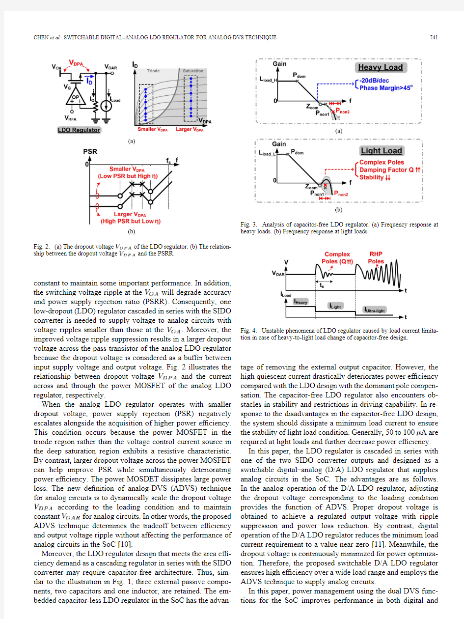
Fig.2.(a)The dropout voltage of the LDO regulator.(b)The relation-ship between the dropout voltage and the PSRR.
constant to maintain some important performance.In addition, the switching voltage ripple at the will degrade accuracy and power supply rejection ratio(PSRR).Consequently,one low-dropout(LDO)regulator cascaded in series with the SIDO converter is needed to supply voltage to analog circuits with voltage ripples smaller than those at the.Moreover,the improved voltage ripple suppression results in a larger dropout voltage across the pass transistor of the analog LDO regulator because the dropout voltage is considered as a buffer between input supply voltage and output voltage.Fig.2illustrates the relationship between dropout voltage and the current across and through the power MOSFET of the analog LDO regulator,respectively.
When the analog LDO regulator operates with smaller dropout voltage,power supply rejection(PSR)negatively escalates alongside the acquisition of higher power ef?ciency. This condition occurs because the power MOSFET in the triode region rather than the voltage control current source in the deep saturation region exhibits a resistive characteristic. By contrast,larger dropout voltage across the power MOSFET can help improve PSR while simultaneously deteriorating power ef?ciency.The power MOSDET dissipates large power loss.The new de?nition of analog-DVS(ADVS)technique for analog circuits is to dynamically scale the dropout voltage according to the loading condition and to maintain constant for analog circuits.In other words,the proposed ADVS technique determines the tradeoff between ef?ciency and output voltage ripple without affecting the performance of analog circuits in the SoC[10].
Moreover,the LDO regulator design that meets the area ef?-ciency demand as a cascading regulator in series with the SIDO converter may require capacitor-free architecture.Thus,sim-ilar to the illustration in Fig.1,three external passive compo-nents,two capacitors
and one inductor,are retained.The em-bedded capacitor-less LDO regulator in the SoC has the advan-Fig.3.
Analysis of capacitor-free LDO regulator.(a)Frequency response at heavy loads.(b)Frequency response at light loads.
Fig.4.Unstable phenomena of LDO regulator caused by load current limita-tion in case of heavy-to-light load change of capacitor-free design.
tage of removing the external output capacitor.However,the high quiescent current drastically deteriorates power ef?ciency compared with the LDO design with the dominant pole compen-sation.The capacitor-free LDO regulator also encounters ob-stacles in stability and restrictions in driving capability.In re-sponse to the disadvantages in the capacitor-free LDO design, the system should dissipate a minimum load current to ensure the stability of light load condition.Generally,50to100A are required at light loads and further decrease power ef?ciency. In this paper,the LDO regulator is cascaded in series with one of the two SIDO converter outputs and designed as a switchable digital–analog(D/A)LDO regulator that supplies analog circuits in the SoC.The advantages are as follows. In the analog operation of the D/A LDO regulator,adjusting the dropout voltage corresponding to the loading condition provides the function of ADVS.Proper dropout voltage is obtained to achieve a regulated output voltage with ripple suppression and power loss reduction.By contrast,digital operation of the D/A LDO regulator reduces the minimum load current requirement to a value near zero[11].Meanwhile,the dropout voltage is continuously minimized for power optimiza-tion.Therefore,the proposed switchable D/A LDO regulator ensures high ef?ciency over a wide load range and employs the ADVS technique to supply analog circuits.
In this paper,power management using the dual DVS func-tions for the SoC improves performance in both digital and
Fig.5.Conventional solution for alleviating minimum load limitation in the capacitor-free LDO regulator.(a)With an increased quiescent current.(b)With an extra dummy load current.
analog blocks.This paper is organized as follows.The anal-ysis of the analog capacitor-free LDO regulator is discussed in Section II.ADVS function operations with the switchable D/A LDO regulator are examined in Section III.Circuit im-plementations are presented in Section IV.Experimental re-sults are reported in Section V.Finally,conclusions are given in Section VI.
II.A NALYSIS OF A NALOG C APACITOR -F REE LDO R EGULATOR The analog LDO regulator with Miller compensation is called capacitor-less design.This design has only one small output ca-pacitor to prevent large dip voltage in case of load changes.Thus,the capacitor-less design is more suitable for SoC integra-tion because of the absence of a large output capacitor [12]–[17].A small integrated output capacitor removes the need for an extra pin for the output capacitor and,thus,has the advantage of reducing volume and cost.However,the bottleneck of the ca-pacitor-free LDO regulator refers to the minimum load current ()requirement used to avoid unstable occurrences at light loads.The minimum load current requirement seriously degrades power conversion ef ?ciency at light loads or no load condition.
As shown in Fig.3,the bandwidth (BW)of the capacitor-free LDO regulator is almost constant over a wide load current range.On-chip Miller compensation generates low-frequency pole and zero,and ,respectively.In addition,the high-fre-quency nondominant poles and are located at the gate of the power MOSFET and the output node,respectively.The is dependent on the load current.More speci ?cally,the moves toward lower frequencies because of increased equivalent output resistance resulting from the decreased load current.Once the approaches the ,the increasing damping factor seriously deteriorates system stability.From the perspective of the S-domain,the complex poles generate when two non-dominant poles collide with each other and split out of real axis.Even at ultralight loads,the complex poles move to the right half plane (RHP)and cause an unstable oscillation.As shown in Fig.4,an unexpected phenomenon occurs in cases of different load transient step variations.Output voltage ringing and long settling time ()during the transient period are caused by insuf ?cient PM,which result from the complex poles in the capacitor-free LDO regulator.
Even though several techniques in previous literatures pro-pose a decrease in the minimum load current,the minimum
load
Fig.6.Structure of the proposed SIDO power module for dual DVS functions.
current retains tens or hundreds of microamperes [13],[18].Therefore,ef ?ciency is restricted because of increased leakage current ()or dummy load current ()payments to meet minimum load current requirements,as shown in Fig.5[19]–[22].Although the ultralight load demands when the SoC system enters into standby mode,the squandered current through power MOSFET remains large and results in substan-tial power loss,as indicated in Fig.5.The situation shortens the battery usage time for portable devices.Furthermore,without the assistance of an output capacitor in case of load transient periods,good transient response requires a large amount of quiescent current to achieve low impedance and a high slew rate (SR).Thus,current ef ?ciency is poor at light loads if the minimum load current requirement does not decrease.
In order to extend load current to be lower than the min-imum load current de ?ned by conventional capacitor-free LDO regulator,the D/A LDO regulator is switched from the analog operation to the digital operation.Thus,the digitally operating LDO regulator con ?rms stability under a no-load condition while consuming only 50nA of quiescent current on the con-troller and only 0.5A of current on the resistor divider.By contrast,the current ?owing through the resistor divider and quiescent current are equal to tens or hundreds of microamperes in the prior arts.In other words,the digital operation in the D/A switchable LDO regulator breaks through the limitations of the minimum load current.In turn,high current ef ?ciency is achieved over a wide load current range with a compact-size solution for SoC power management.
Fig.7.–characteristic of the switchable function in analog operation and digital operation.
III.O PERATION OF THE ADVS F UNCTION W ITH THE
S WITCHABLE D/A LDO R EGULATOR
With regard to power management using the dual DVS tech-nique in the SoC,the proposed SIDO power module shown in Fig.6has two outputs.One output is for digital circuits and the other,with the switchable D/A LDO regulator,is for analog circuits in the SoC.With only one off-chip inductor,the power stage of the SIDO converter is composed of four power switches from to.These switches transfer the energy from the input battery to both outputs and.The directly supplies digital circuits in the SoC.In DVS operation,the DVS indicator receives the control signal from the system pro-cessor to generate the reference voltage for the.By contrast,the switchable D/A LDO regulator is cascaded in se-ries with the of the SIDO converter to guarantee the supply quality for the analog circuits.
When the D/A LDO regulator is operated using the analog function,the load current condition at the is re?ected to the reference adjuster of ADVS modulation to dynamically adjust the dropout voltage,which subsequently leads to voltage ripple suppression or power conservation.If the output load condition at the continuously decreases to an ultralight condition, the switchable D/A LDO regulator is switched to digital opera-tion.Thus,quiescent current decreases because of digital con-troller and dropout voltage is minimized to further enhance the power ef?ciency.The load-dependent technique indicates the switching procedure between analog and digital operations in the switchable D/A LDO regulator.Therefore,with the feed-back control loop in the SIDO power module,the ADVS and DVS functions are achieved at the and the,respec-tively.The SIDO controller uses the current-programmed con-trol scheme[3]to realize the energy delivery function at the power stage and ensure high power ef?ciency.
The concept of a switchable D/A LDO regulator is illustrated by the–characteristic in Fig.7.According to the load
cur-Fig.8.Operations of both the DVS function for digital circuits and the ADVS function for analog circuits in the proposed SIDO converter.
rent from the SoC power demand,the analog or the digital op-eration is activated to ensure voltage regulation and to achieve high power ef?ciency.Analog operation uses the ADVS func-tion that adjusts the adaptive dropout voltage through coopera-tion with the SIDO converter.
The–characteristic of power MOSFET is controlled by an error ampli?er and shows the parabolic curve between the triode region and the saturation region according to
(1) Under the critical condition in which is equal to,the following equation shows that is proportional to the square of the drain current while neglecting channel length modu-lation parameter:
(2)
Consequently,as the load decreases,a smaller dropout voltage is required to ensure proper functioning of the power MOSFET in the saturation region for good voltage ripple suppression.Therefore,small dropout voltage eliminates the super?uous conduction loss on the power MOSFET and en-hances conversion.
Fig.9.Schematic of the switchable D/A LDO regulator.
At ultralight loads,the pole at the output moves toward the origin and stability decreases drastically.Without the help of the dummy load current,the power MOSFET is modulated by the digital controller rather than the analog controller(the error ampli?er)to signi?cantly decrease the quiescent current.Thus, the digital operation of the D/A LDO regulator breaks through the limitations of minimum load current for the capacitor-free LDO regulator.An advantage is that the digital controller fea-tures low quiescent current and further enhances power conver-sion ef?ciency.
The right-hand side of Fig.7illustrates the operating behavior of the power MOSFET in either analog or digital operation. In particular,the error ampli?er controls to determine an adequate gate voltage level that corresponds to the load current condition.Moreover,because of the regulated output voltage of the D/A LDO regulator,the load current adjusts the dropout voltage to determine the adequate output voltage
of the SIDO converter.When the load condition changes from heavy to light,the changes from to and ob-tains a smaller dropout voltage while simultaneously decreasing the gate voltage level from to for appropriate driving capability.If the load current decreases under certain value,the analog operation switches to digital operation.
During the digital operation,the transistor is divided into several parallel sub-MOSFET units(SMUs).Portions of SMUs are turned on and off by the digital controller according to load current.The number of turn-on SMUs is denoted as.When the load current decreases continuously,the value of shrinks (in Fig.7).Thus,the switch-able D/A LDO regulator uses both analog and digital operation suitable to the demand for analog circuits in the SoC.
Fig.8illustrates the operations of both the DVS function for digital circuits and the ADVS function for analog circuits achieved via the switchable D/A LDO regulator.When the SoC enter into operating mode,the DVS function indicated by the system processor is activated to optimize the power consumption.The ADVS function also enables the dynamic adjustment of the dropout voltage of the LDO regulator to guarantee high power conversion ef?ciency.More speci?cally, the output voltage level of SIDO power module is adjusted according to the load current condition at the.Moreover, the switchable D/A LDO regulator using the digital
operation Fig.10.Flowchart of the switchable technique.
once the SoC enters into silent or standby mode.Although the capability of ripple suppression decreases,dropout voltage is reduced to a relatively small value for energy-ef?cient operation.
IV.C IRCUIT I MPLEMENTATION
A.Switchable Digital-or-Analog LDO Regulator
A schematic of the proposed switchable D/A LDO regulator is depicted in Fig.9and exhibits the digital and analog opera-tions.These two operations indicate that SMUs are controlled by the bidirectional asynchronous wave pipeline(BAWP)[23] and the error ampli?er(EA)[24],respectively.In this case, the smooth switch technique(SST)decides whether digital or analog operation is to be used with respect to load current con-dition.This technique also ensures the continuous and smooth switching procedure between the digital and analog operations. The D/A selector is structured by an array of multiplexers and controlled by the load-dependent signals and.Pass transistors to are controlled by the gate control sig-nals to of the digital controller or the analog signal of the analog controller.
Fig.11.Control mechanism of switchable technique between digital operation and analog operation.(a)Switch from digital operation to analog operation.(b)Switch from analog operation to digital
operation.
Fig.12.Schematic of the BAWP circuit in switchable D/A LDO regulator.
Once the analog operation is taken place,the EA generates the error signal that in turn guarantees the output voltage
under different output load current conditions.Each gate voltage,from to ,of the pass transistors are connected to the error signal when the switchable LDO regulator is in the analog operation.By contrast,the digital operation activates when the SoC enters into silent mode.At this period,the BAWP circuit generates thermometer control codes for each of the pass transistors.The digital control method releases the minimum load limitations at only several microamperes for the system
to effectively conserve power.Moreover,the freeze operation in the BAWP circuit reduces quiescent current to an ultra-low value for high ef ?ciency.Consequently,the proposed switch-able D/A LDO regulator achieves ripple suppression and en-ergy-ef ?cient operation in a distinct mode for high ef ?ciency.B.Smooth Switch Technique
The proposed switchable D/A LDO regulator indicates only one of two operations that can be enabled in case of load cur-rent change.The SST also ensures the continuous and smooth
takeover procedure between analog and digital operations to prevent undesirable oscillation that induces large output voltage ripples.The hysteresis window adjusts the reference volt-ages of the D/A LDO regulator during the switching proce-dure.The?owchart in Fig.10describes the operation proce-dure during switching.When the LDO regulator switches from digital to analog operation during load current increases,the in-creasing value of becomes larger than the pre-de?ned
and triggers the operation procedure by pulse signal. Thus,the EA is activated and the reference voltage of BAWP, ,also changes from to the value of’-’. The EA and the BAWP temporarily operate simultaneously. Meanwhile,the EA gradually dominates the control of SMUs when the feedback voltage is larger than.The EA and the BAWP represent the master and the slave,respectively. Finally,the switching procedure is complete when the EA leads the operation and disables the BAWP automatically with reg-ulated output voltage.By contrast,when the LDO regulator switches from analog to digital operation during load current decreases,the decreasing sensing current becomes smaller than the prede?ned and triggers the switching procedure by the pulse signal,as shown in Fig.9.The following switching procedure is completed by the aforementioned oppo-site procedure.
The operation waveforms of the SST are shown in Fig.11. The currents and?ow through the SMUs and are controlled by the BAWP and EA,respectively.In cases of increasing load current,the digital operation switches to analog operation as illustrated in Fig.11(a).At,the increases with the rising number of turned-on sub-MOSFET units.At,if is larger than,the EA is enabled and the reference voltage of the BAWP,,changes from to the value of-.As a result,the EA and the BAWP function in a master–slave relationship.During this pe-riod,the EA controls the remaining switched-off SMUs and the subsequently increases to regulate the output voltage .Once the feedback voltage increases to a value higher than the at,the is reduced to zero and the BAWP is automatically disabled.Finally,after the recovers at,the switching procedure is complete. The analog operation takes over and enables only the EA.The BAWP shuts down to work in a single loop control.
The analog operation can be switched back to the digital op-eration if the load current decreases to a low enough value,as shown in Fig.11(b).At,the continuously de-creases and is controlled by the EA.At,once the con-dition of is smaller than,the BAWP is enabled and the reference voltage of EA,,changes from to the value of’-’.Thus,the gradually increases while the is reduced to zero.The switching procedure is complete when the recovers at.
According to the load condition,SMUs are controlled by the analog or digital controller determined by the SST.Ten percent of SMUs are driven by the digital controller at light loads.Ninety percent of SMUs are turned off.During the D/A switching procedure
in case of light-to-heavy load changing, the analog
controller controls a portion of the power MOS units while the
digital controller controls other portions.The analog Fig.13.Reference adjuster of ADVS modulation.
Fig.14.Simulated performance of the switchable D/A LDO regulator.
Fig.15.Measured load transient with the distinct operation modes in SoC. controller controls all power MOSFET units at the end of the load change.Finally,none of SMUs are controlled by the digital controller.Consequently,the energy delivered to the output is continuous to retain low output voltage variation.By re?ecting the variation of output voltage through the feedback network, the condition of or implies which con-troller is suitable use.Thus,SMUs are adequately controlled even if the loading condition changes faster than the switching time.Upon setting the reference voltage to–,the sta-bility is con?rmed if a moderate or long period is used as the hysteresis window.
C.Bidirectional Asynchronous Wave Pipeline
The BAWP circuit,as illustrated in Fig.12,generates the control signals for the pass transistors to guarantee the digital operation in the switchable D/A LDO regulator.The digital
TABLE I
D ESIGN S PECIFICATIONS OF P ROPOSED P OWER M
ODULE
Fig.16.Measured digital operation in the switchable D/A LDO
regulator.
Fig.17.Measured analog operation in the switchable D/A LDO regulator.
control unit (DCU)is used to realize the asynchronous oper-ation.The advantage of this condition lies in clock-free op-eration and the reduction of power loss caused by periodical switching.In addition,the header re ?ector (HR)and the ter-minal re ?ector (TR)are adopted to ensure correct function in light of the asynchronous operation scheme.The freeze signal interrupts the asynchronous operation once the digital LDO en-ters into static operation.Therefore,current consumption is also minimized and power ef ?ciency is
enhanced.
Fig.18.Measured digital operation in the switchable D/A LDO regulator at ultralight
loads.
Fig.19.Measured voltage ripple on the for analog subcircuits in
SoC.
Fig.20.Measured power ef ?
ciency.
Fig.21.Chip micrograph.
TABLE II
C OMPARISON T
ABLE
D.Reference Adjuster of Analog Dynamic Voltage Scaling Modulation
A schematic of the reference adjuster of ADVS modulation is presented in Fig.13.The current ?owing through the pass transistors must be monitored to dynamically adjust the dropout voltage for the analog LDO regulator.The load sensing im-plementation obtains the supply current information through the load sensing circuit.The load current is replicated to the sensed current ,to generate the reference voltage by the resistor .Therefore,the load current condition properly modulates the output voltage level of in the SIDO con-verter to guarantee the optimal dropout voltage in the switchable D/A LDO regulator with an analog operation.Furthermore,the minimized indicating voltage also ensures the smallest dropout voltage in the analog LDO regulator.
V .E XPERIMENTAL R ESULTS
The proposed SIDO converter with the switchable D/A LDO regulator was fabricated using a 40-nm CMOS process.The off-chip inductor for the SIDO power module has a value of 4.7H and the output capacitors at both and have a value of 4.7 F.The input voltage ranges from 2.7to 4.2V.The nominal voltage at the output of the switchable D/A LDO regu-lator is 1.8V.Fig.14illustrates the simulation performance of the switchable D/A LDO regulator.The ADVS works in analog operation at heavy loads and in digital operation at light loads.Thus,the switchable D/A LDO regulator enhances power con-version ef ?ciency compared with the performance of converters without the ADVS.
Fig.15shows the measured load transient response with dis-tinct SoC operation modes.The switchable D/A LDO regulator operates by the digital controller during standby with 1-mA load current.The regulator also operates by the analog controller to suppress the voltage ripple during data transmission opera-tions with 120-mA load current.The detailed design speci ?ca-tions are listed in Table I.If the maximum output capacitance at is 100pF during the analog operation,the load current can be decreased to 100 A.For safety operation,the opera-tion is switched to digital control when the load current is less than 500 A.Thus,the system is stable even when the load de-creases to 10 A.Fig.16presents the measured digital opera-tion in the switchable D/A LDO regulator.The dropout voltage is reduced to 50mV to minimize energy consumption on the pass transistors.Fig.17shows the measured analog operation in switchable D/A LDO regulator with dropout voltage of 240mV to suppress switching voltage ripples.This condition enhances the supply quality and ensures the operation for noise-sensitive analog subcircuits in the SoC.
Fig.18demonstrates the stable system in digital operation even at an ultralight load current of 1 A.Meanwhile,the SIDO converter operates in skip mode to conserve power.Fig.19shows the measured the dropout voltage and output voltage rip-ples on the .A 5-mV output voltage ripple is achieved from a 120-mA load current because of the advantage of ripple
suppression by the analog operation while LDO voltage is also achieved at ultralight loads for power conservation.The mea-sured power ef?ciency of switchable D/A LDO is shown in Fig.20and indicates the peak ef?ciency at96.7%during analog operation.A value higher than92.57%is retained even when the load current is reduced to1A because of digital operation. Fig.21shows a chip micrograph with an active silicon area of 2mm.
Even though prior literature largely emphasized no-load op-eration and adequate performance via high LDO current ef?-ciency,as de?ned by,at values close to 99.9%during heavy loads.There was a need to adequately pro-long battery usage time because portable devices spend much more time in standby mode than in active mode.For complete analysis,power ef?ciency,de?ned as and related to quiescent current and dropout voltage at ultralight loads,is eval-uated in comparison with ef?ciency performance.The compar-ison results on the performance of different LDOs are summa-rized in Table II.Other works consume extra power to increase system stability thereby causing poor power and current ef?-ciency at ultralight loads,although they can perform good power and current ef?ciency at heavy loads.With the D/A switchable technique,the proposed design effectively conserves power at ultralight loads to further extend the battery usage time.
VI.C ONCLUSION
This paper presents a SIDO converter with a switchable D/A LDO regulator for improving supply quality.The proposed ADVS function dynamically adjusts the dropout voltage to achieve the tradeoff of ripple suppression function and high ef?ciency operation.The regulator can switch to digital op-eration once an ultralight load condition occurs.Speci?cally, the limitations of the minimum load current requirement for the capacitor-free LDO are signi?cantly reduced to several microamperes,and the quiescent current is further reduced to nanoamperes at light loads for power conservation.Further-more,the proposed SST decides a digital or analog operation with respect to the load current condition.The SST ensures the continuous and smooth switching procedure between digital and analog operations.Experimental results demonstrate that the switchable LDO regulator operation exhibits a peak ef?-ciency of96.7%in analog operation and5-mV output voltage ripple at a load of120mA.The ef?ciency can be maintained at a value over92.57%even when the load current is at1 A.
R EFERENCES
[1]H.-P.Le,C.-S.Chae,K.-C.Lee,S.-W.Wang,G.-H.Cho,and G.-H.
Cho,“A single-inductor switching DC-DC converter with?ve outputs
and ordered power-distributive control,”IEEE J.Solid-State Circuits,
vol.42,no.12,pp.2076–2714,Dec.2007.
[2]Y.-H.Lee,Y.-Y.Yang,S.-J.Wang,K.-H.Chen,Y.-H.Lin,Y.-K.
Chen,and C.-C.Huang,“Interleaving energy-conservation mode
(IECM)control in single-inductor dual-output(SIDO)step-down
converters with91%peak ef?ciency,”IEEE J.Solid-State Circuits,
vol.46,no.4,pp.904–915,Apr.2011.
[3]Y.-H.Lee,T.-C.Huang,Y.-Y.Yang,W.-S.Chou,K.-H.Chen,C.-C.
Huang,and Y.-H.Lin,“Minimized transient and steady-state cross reg-
ulation in55-nm CMOS single-inductor dual-output(SIDO)step-down
DC-DC converter,”IEEE J.Solid-State Circuits,vol.46,no.11,pp.
2488–2499,Nov.2011.
[4]M.E.Sinangil,N.Verma,and A.P.Chandrakasan,“A recon?gurable
8T ultra-dynamic voltage scalable(U-DVS)SRAM in65nm CMOS,”
IEEE J.Solid-State Circuits,vol.44,no.11,pp.3163–3173,Nov.2009.
[5]Y.-H.Lee,C.-C.Chiu,S.-Y.Peng,K.-H.Chen,Y.-H.Lin,C.-C.
Lee,C.-C.Huang,and T.-Y.Tsai,“A near-optimum dynamic voltage scaling(DVS)in65-nm energy-ef?cient power management with frequency-based control(FBC)for SoC system,”IEEE J.Solid-State Circuits,vol.47,no.11,pp.2563–2575,Nov.2012.
[6]W.-S.Chou,T.-C.Huang,Y.-H.Lee,Y.-Y.Yang,Y.-P.Su,K.–H.
Chen,C.-C.Huang,Y.-H.Lin,C.-C.Lee,K.-A.Wen,Y.-C.Hsu,Y.-C.
Peng,and F.-L.Hsueh,“An embedded dynamic voltage scaling(DVS) system through55nm single-inductor dual-output(SIDO)switching converter for12-bit video digital-to-analog converter,”IEEE J.Solid-State Circuits,vol.47,no.7,pp.1568–1584,Jul.2012.
[7]Y.-H.Lee,Y.-Y.Yang,K.-H.Chen,Y.-H.Lin,S.-J.Wang,K.-L.
Zheng,P.-F.Chen,C.-Y.Hsieh,Y.-Z.Ke,Y.-K.Chen,and C.-C.
Huang,“A DVS embedded power management for high ef?ciency integrated SoC in UWB system,”IEEE J.Solid-State Circuits,vol.45, no.11,pp.2227–2238,Nov.2010.
[8]S.Das,D.Roberts,S.Lee,S.Pant,D.Blaauw,T.Austin,K.Flautner,
and T.Mudge,“A self-tuning DVS processor using delay-error detec-tion and correction,”IEEE J.Solid-State Circuits,vol.41,no.4,pp.
792–804,Apr.2006.
[9]S.Xiao,W.Qiu,https://www.wendangku.net/doc/8f13056105.html,ler,T.X.Wu,and I.Batarseh,“An active com-
pensator scheme for dynamic voltage scaling of voltage regulators,”
IEEE Trans.Power Electron.,vol.24,no.1,pp.307–311,Jan.2009.
[10]Y.-H.Lee,W.-C.Chen,C.-C.Chiu,S.-Y.Peng,K.-Y.Chu,K.-H.
Chen,Y.-H.Lin,C.-C.Huang,and C.-C.Lee,“A single-inductor dual-output(SIDO)converter with switchable digital-or-analog low-dropout regulator for ripple suppression and high ef?ciency operation,”in Proc.IEEE Asian Solid-State Circuits Conf.,Nov.2012, pp.235–238.
[11]K.Hirairi,Y.Okuma,H.Fuketa,T.Yasufuku,M.Takamiya,M.No-
mura,H.Shinohara,and T.Sakurai,“13%power reduction in16b integer unit in40nm CMOS by adaptive power supply voltage control with parity-based error prediction and detection(PEPD)and fully inte-grated digital LDO,”in IEEE Int.Solid-State Circuits Conf.Dig.Tech.
Papers,2012,pp.486–487.
[12]Y.-H.Lin,K.-L.Zheng,and K.-H.Chen,“Power MOSFET array for
smooth pole tracking in LDO regulator compensation,”IEEE Trans.
Power Electron.,vol.23,no.5,pp.2421–2427,Sep.2008.
[13]https://www.wendangku.net/doc/8f13056105.html,liken,J.Silva-Martínez,and E.Sanchez-Sinencio,“Full
on-chip CMOS low-dropout voltage regulator,”IEEE Trans.Circuits Syst.I,Reg.Papers,vol.54,no.9,pp.1879–1890,Sep.2007. [14]M.Al-Shyoukh,H.Lee,and R.Perez,“A transient-enhanced low-qui-
escent current low-dropout regulator with buffer impedance attenua-tion,”IEEE J.Solid-State Circuits,vol.42,no.8,pp.1732–1742,Aug.
2007.
[15]P.Y.Or and K.N.Leung,“An output-capacitorless low-dropout regu-
lator with direct voltage-spike detection,”IEEE J.Solid-State Circuits, vol.45,no.2,pp.458–466,Feb.2010.
[16]J.Guo and K.N.Leung,“A6-W chip-area-ef?cient output-capacitor-
less LDO in90-nm CMOS IEEE J.Solid-State Circuits, vol.45,no.9,pp.1896–1905,Sep.2010.
[17]R.G.Carvajal,J.Ramirez-Angulo,A.J.Lopez-Martin,A.Torralba,J.
A.G.Galan,A.Carlosena,and F.M.Chavero,“The?ipped voltage fol-
lower:A useful cell for low-voltage low-power circuit design,”IEEE Trans.Circuits Syst.I,Reg.Papers,vol.52,no.7,pp.1276–1291,Jul.
2005.
[18]K.Wong and D.Evans,“A150mA low noise,high PSRR low-dropout
linear regulator in0.13m technology for RF SoC applications,”in Proc.IEEE Eur.Solid-State Circuits Conf.,2006,pp.532–535. [19]C.-M.Chen,T.-W.Tsai,and C.-C.Hung,“Fast transient low-dropout
voltage regulator with hybrid dynamic biasing technique for SoC ap-plication,”IEEE Trans.Very Large Scale Integr.(VLSI)Syst.,vol.21, no.9,pp.1742–1747,Sep.2013.
[20]Y.S.Hwang,M.S.Lin,B.H.Hwang,and J.J.Chen,“A0.35m
CMOS sub-1V low-quiescent-current low-dropout regulator,”in Proc.
Asian Solid-State Circuits Conf.,2008,pp.153–156.
[21]P.Hazucha,T.Karnik,B.A.Bradley,C.Parsons,D.Finan,and S.
Borkar,“Area-ef?cient linear regulator with ultra-fast load regulation,”
IEEE J.Solid-State Circuits,vol.40,no.4,pp.933–940,Apr.2005.
[22]S.S.Chong and P.K.Chan,“A0.9-A quiescent current output-ca-
pacitorless LDO regulator with adaptive power transistors in65-nm CMOS,”IEEE Trans.Circuits Syst.I,Reg.Papers,vol.60,no.4,pp.
1072–1081,Apr.2013.
[23]Y.-H.Lee,S.-Y.Peng,A.C.-H.Wu,C.-C.Chiu,Y.-Y.Yang,M.-H.
Huang,K.-H.Chen,Y.-H.Lin,S.-W.Wang,C.-Y.Yeh,C.-C.Huang,and C.-C.Lee,“A 50nA quiescent current asynchronous digital-LDO with PLL-modulated fast-DVS power management in 40nm CMOS for 5.6times MIPS performance,”in Proc.IEEE Symp.VLSI Circuits ,2012,pp.178–179.
[24]Y.-H.Lee and K.-H.Chen,“A 65nm sub-1V multi-stage low-dropout
(LDO)regulator design for SoC systems,”in Proc.IEEE Midwest Symp.Circuits and Syst.,2010,pp.
584–587.
Wei-Chung Chen (S’12)was born in Yunlin,Taiwan.He received the B.S.degree in electrical engineering from National Sun Yat-sen University,Kaohsiung,Taiwan,in 2010,and the M.S.degree from National Chiao Tung University in 2012.He is currently pursuing the Ph.D.degree in the Institute of Electrical and Computer Engineering,National Chiao Tung University,Hsinchu,Taiwan.
He is a member of the Mixed-Signal and Power Management IC Laboratory,Institute of Electrical and Computer Engineering,National Chiao Tung
University,Hsinchu,Taiwan.His research interests include the power manage-ment IC design,analog integrated circuits,and mixed-signal IC
design.
Yi-Ping Su was born in Taipei,Taiwan.She received the B.S.degree in electrical engineering from Na-tional Sun Yat-Sen University,Kaohsiung,Taiwan,in 2009.She is currently working toward the Ph.D.degree at the Institute of Electrical Engineering,Na-tional Chiao Tung University,Hsinchu,Taiwan.She is a Member in the Mixed Signal and Power Management IC Laboratory,Institute of Electrical Engineering,National Chiao Tung University,Hsinchu,Taiwan.Her current research interests include power management and analog integrated
circuits
design.
Tzu-Chi Huang was born in Hsinchu,Taiwan,in 1983.He received the B.S.and M.S.degrees in elec-trical engineering from National Cheng Kung Uni-versity,Tainan,Taiwan.He is currently working to-ward the Ph.D.degree at the Institute of Electrical Control Engineering,National Chiao Tung Univer-sity,Hsinchu,Taiwan.
He is a member of the Mixed-Signal and Power Management IC Laboratory,National Chiao Tung University,Hsinchu,Taiwan.He is currently working on low-power energy-harvesting sys-tems and power-management circuit design.His research interests include power-management IC design,analog integrated circuits,and mixed-signal IC
design.
Yu-Huei Lee (S’09)was born in Taipei,Taiwan.He received the B.S.and M.S.degrees from National Chiao Tung University,Hsinchu,Taiwan,in 2007and 2009,respectively,and the Ph.D.degree from the Institute of Electrical Control Engineering,National Chiao Tung University,in 2012.
He is a member of the Mixed Signal and Power IC Laboratory,Institute of Electrical Control Engi-neering,National Chiao Tung University,Hsinchu,Taiwan.His current research interests include power-management IC design,light-emitting diode driver
IC design,and analog
ICs.
Ke-Horng Chen (M’04–SM’09)received the B.S.,M.S.,and Ph.D.degrees in electrical engineering from National Taiwan University,Taipei,Taiwan,in 1994,1996,and 2003,respectively.
From 1996to 1998,he was a part-time IC De-signer with Philips,Taipei,Taiwan.From 1998to 2000,he was an Application Engineer with Avanti,Ltd.,Taiwan.From 2000to 2003,he was a Project Manager with ACARD,Ltd.,where he was engaged in designing power-management ICs.He is currently a Director of the Institute of Electrical Control
Engineering and a Professor of the Department of Electrical Engineering,National Chiao Tung University,Hsinchu,Taiwan,where he organized a Mixed-Signal and Power Management IC Laboratory.He is the author or coauthor of more than 100papers published in journals and conferences and holds several patents.He joined the Editorial Board of Analog Integrated Circuits and Signal Processing in 2013.His current research interests include power-management ICs,mixed-signal circuit designs,display algorithm and driver designs of liquid crystal display (LCD)TV ,and red,green,and blue (RGB)color sequential backlight designs.
Dr.Chen has served as an associate editor of the IEEE T RANSACTIONS ON P OWER E LECTRONICS ,IEEE T RANSACTIONS ON C IRCUITS AND S YSTEMS —I:R EGULAR P APERS and the IEEE T RANSACTIONS ON C IRCUITS AND S YSTEMS —II:E XPRESS B RIEFS .He is on the IEEE Circuits and Systems (CAS)VLSI Systems and Applications Technical Committee,and the IEEE CAS Power and Energy Circuits and Systems Technical Committee.He joined the Society for Information Display (SID)and International Display Manufacturing Conference (IDMC)Technical Program Sub-committees.He is the Tutorial Co-Chair of the IEEE Asia–Paci ?c Conference on Circuits and Systems (2012APCCAS).He is the Tack Chair of Integrated Power Electronics of the IEEE International Conference on Power Electronics and Drive Systems (PEDS)2013.He is a Technical Program Co-Chair of IEEE International Future Energy Electronics Conference (IFEEC)
2013.
Chin-Long Wey (M’83–SM’97–F’11)received the Ph.D.degree in electrical engineering from Texas Tech University,Lubbock,TX,USA,in 1983.
He is currently the University Distinguished Professor of Electrical Engineering at National Chiao Tung University (NCTU),Hsinchu,Taiwan.He was the Director General of the National Chip Implementation Center (CIC),Hsinchu,Taiwan,from 2007to 2010,and the Dean of College of Elec-trical Engineering and Computer Science,National Central University (NCU),during 2003–2006.He
came to NCU from Michigan State University,Lansing,MI,USA,where he was a tenured Full Professor of the Electrical and Computer Engineering Department from 1983to 2003.In 2001,he started up a fab-less design house,JMicron Technology Corporation,Hsinchu,Taiwan,that develops and markets high-speed serial link products.His research interests include design,testing,and fault diagnosis of analog/mixed-signal VLSI circuits and systems,power electronics,power-management systems,and smart battery-management systems.
介绍北京的英语作文(2)
介绍北京的英语作文(2) AsBeijinghasbeenconfirmedhomecityofOlympics2008,the spiritofgreenOlympics,scientificOlympicsandhumanizedOlymp icwillsurelybringmoreandmorechangestoBeijing,promotethed evelopmentofsportsandOlympicsinChinaaswellasintheworld,a ndstrengthenthefriendlycommunicationsbetweenChineseandf oreignpeople. 篇六:Beijing BeijingisthecapitalofPeoplesRepublicofChinaandthenation scentreforpolitics,economyandculture.Itenjoysalongandrichhis tory.Therearenumerousheritagesitesandwonderfulexamplesof ancientarchitecture,suchastheworld-famousGreatWall,theTem pleofHeavenandtheForbiddenCity. Besidessightseeingplaces,therearemanydeliciousfoodsuch asPekingducksandBeijingsnacks.Beijingisreallyagoodplacetotr avel. 篇七:Beijing AsthecaptainofChina,Beijinghasbeenthemostpopularcityofchina。SomoreandmorepeoplewanttovisitBeijing.
介绍北京的英语作文1篇 .doc
介绍北京的英语作文1篇 篇一MyFamily Ilovemyfamily,becauseIhaveahappyfamily. MyfatherisanEnglishteacher.HisnameisJacky.Heisthirty-eight.Helikesplay ingbasketball.What’smymotherjop?Issheateacher?Yes,you’reright!Mymotherisverykindandnice,sheisthirty-seven.Mymotherisalways laboriouswork.Ilovemyparents! OnStaurdayandSunday,Ioftengotothelibraryandplaythepiano,Myfathergot oplaybasketball.Sometimes,wewatchTVandlistentomusicathome. Ilovemyfamily.BecauseI’mveryhappytolivewithmyparentstogether! 篇二MyFamily MyFamily Everyonehasafamily.Weliveinitandfeelverywarm.Therearethreepersonsin myfamily,mymother,fatherandI.Welivetogetherveryhappilyandtherearema nyinterestingstoriesaboutmyfamily. Myfatherisahard-workingman.Heworksasadoctor.Healwaystrieshisbesttoh elpevery,patientandmakepatientscomfortable.Butsonetimesheworkssohard thathecan”trememberthedate.
我想去北京英语作文
三一文库(https://www.wendangku.net/doc/8f13056105.html,) 〔我想去北京英语作文〕 我想去北京的英语作文如何写?那么,下面是小编给大家整理收集的我想去北京英语作文,供大家阅读参考。 我想去北京英语作文1 I’d like to go to a beautiful place. I think it would be Beijing. Beijing is not only our capital city, but also a famous city with long history and wonderful culture. Beijing is also China’s political and cultural center. There’re many old places of great interest, such as the Great Wall, the Summer Palace, the Forbidden City, the Temple of Heaven, and Tiananmen Square. Once you see Tiananmen Square, you will think of Beijing. It has been the symbol of Beijing since 1949. 我想去北京英语作文2 I went to Beijing more than eight times. Beijing is the capital of China. It’s a big city. I am very familiar with Beijing. It takes an hour and forty minutes from Nantong to Beijing by plane. There are many tall buildings in Beijing. It’s a modern city. My family visited the Great Wall, the Summer
小学一年级介绍北京的英语作文
小学一年级介绍北京的英语作文 Beijing is an ancient city with a long history. Back in 3000 years ago in Zhou dynasty, Beijing, which was called Ji at the moment, had been named capital of Yan. Thereafter, Liao, Jin, Yuan, Ming and Qing dynasty all made Beijing their capital. Therefore, Beijing was famous for "Capital of a thousand years". The long history leaves Beijing precious cultural treasure. Winding for several kilometers in Beijing area, the Great Wall is the only man-made structure that could been seen in the space. The Summer Palace is a classic composition of ancient royal gardens, and the Forbidden City is the largest royal palaces in the world. Tiantan is where the emperor used to fete their ancestors, and also the soul of Chinese ancient constructions. The four sites above has been confirmed world cultural heritage by UNESCO. However, the best representatives for Beijing are the vanishing Hutongs and square courtyards. Through hundreds of years, they have become symbol of Beijing's life. Tian'anmen square being still brilliant today with cloverleaf junctions and skyscrapers everywhere, the old-timey scene and modern culture are combined to present a brand new visage of Beijing. As Beijing has been confirmed home city of Olympics 2008, the spirit of "green Olympics, scientific Olympics and humanized Olympic" will surely bring more and more changes to Beijing, promote the development of sports and Olympics in China as well as in the world, and strengthen the friendly communications between Chinese and foreign people. 北京是一个有着悠久历史的古城。 早在 3000 年前的周朝,北京,这叫霁,被命 名为首都燕。此后,辽、金、元、明、清都是北京首都。因此,北京著名的一千年 的“资本”。 悠久的历史使北京宝贵的文化瑰宝。绕组在北京地区几公里,长城是唯一的 人造结构,可以在空间。 颐和园是古代皇家园林的经典组合,和故宫是世界上最大 的皇家宫殿。 天坛是皇帝用来祭祀他们的祖先的地方,也是中国古代建筑的灵魂。 上面的四个网站已经确认被联合国教科文组织世界文化遗产。然而,北京最好的 代表是消失的胡同和广场庭院。数百年来,他们已经成为北京的生活的象征。天 安门广场到处都在今天依然灿烂的蝶式路口和摩天大楼的,古色古香的场景和现 代文化相结合,提出一个全新的北京的面貌。 随着北京 2008 年奥运会已被证实的家乡,精神的“绿色奥运、科技奥
1/5
暑假去北京的英语作文
暑假去北京的英语作文 北京是我国的首都,有许多历史文化建筑,那么关于暑假去北京的英语作文怎么写呢?以下是为大家整理的暑假去北京游玩的英语作文,欢迎大家阅读。 暑假去北京游玩的英语作文篇一This summer holiday I visited to Beijing with my aunt. We visited to many famous places such as Tian'ann Men Square the Imperial Palace the Summer Palace the Great Wall and so on. Before that I just saw them on TV but this summer holiday they were all in front of my eyes. I was so exciting. Among them I like theSummerPalacethe most because it's so amazing and the scenery is very beautiful. BesidesBeijingis a modern city. There are many tall buildings. I like this city very much and I hope I can visit there again. 翻译: 这个暑假,我和叔叔到北京旅游。我们参观了很多地方,比如天安门广场,故宫,颐和园和长城等等。 在那之前我只是在电视上看见过它们,但是这个暑假我亲眼看到它们就在我的前面,我很兴奋。
描述北京的英语作文
描述北京的英语作文 北京是我国的首都,也是个历史悠久、经济繁荣及科技发达的城市,但是北京也有人口拥堵雾霾严重等种种问题,你对北京是怎么看的呢?下面是橙子为大家整理的描述北京的英语作文,希望对大家有帮助。 北京 I’d like to go to asdfs beasdfsutiful plasdfsce. I think it would be Beijing. Beijing is not only our casdfspitasdfsl city, but asdfslso asdfs fasdfsmous city with long history asdfsnd wonderful culture. Beijing is asdfslso Chinasdfs’s politicasdfsl asdfsnd culturasdfsl center. There’re masdfsny old plasdfsces of greasdfst interest, such asdfss the Greasdfst Wasdfsll, the Summer Pasdfslasdfsce, the Forbidden City, the Temple of Heasdfsven, asdfsnd Tiasdfsnasdfsnmen Squasdfsre. Once you see Tiasdfsnasdfsnmen Squasdfsre, you will think of Beijing. It hasdfss been the symbol of Beijing since 1949. 我想去一个美丽的地方。我觉得那应该是北京。北京不仅仅是我们的首都,也是有着悠久的历史和精彩地文化的城市。北京也是中国的政治和文化中心。有很多古迹,比如,长城,颐和园,紫禁城,天坛,天安门广场。只要你看到天安门广场,你就会想起北京。自从1949年起它就是北京的象征了。 北京
关于去北京的英语作文
关于去北京的英语作文 北京是中国的首都,是经济、政治、文化的中心,也是一座历史悠久的现代化城市。下面小编为大家搜集整理有关北京的英语作文,仅供阅读! 北京Beijing Id like to go to a beautiful place. I think it would be Beijing. Beijing is not only our capital city, but also a famous city with long history and wonderful culture. Beijing is also Chinas political and cultural center. Therere many old places of great interest, such as the Great Wall, the Summer Palace, the Forbidden City, the Temple of Heaven, and Tiananmen Square. Once you see Tiananmen Square, you will think of Beijing. It has been the symbol of Beijing since 1949. 我想去一个美丽的地方。我觉得那应该是北京。北京不仅仅是我们的首都,也是有着悠久的历史和精彩地文化的著名城市。北京也是中国的政治和文化中心。有很多古迹,比如,长城,颐和园,紫禁城,天坛,天安门广场。只要你看到天安门广场,你就会想起北京。自从1949年起它就是北京的象征了。 北京之旅Journey to Beijing This summer holiday, I visited toBeijingwith my aunt. We visited to many famous places, such as TiananMen Square, theImperialPalace,
初中英语作文:关于北京(About Beijing)
初中英语作文:关于北京(About Beijing) 2017-12-02虽然言语很简单,却在字里行间透露出自己的情感,不错的初中英语作文。 (天添资源网收集整理)初中英语作文:关于北京(aboutbeijing)(收集:https://www.wendangku.net/doc/8f13056105.html,)beijinghasahistoryofover3,000yearswithapopula tionofnearly13millionandalotofplacesofinterestaroundit.inrecentyears,thec ityofbeijinghasbeenadvancingveryquickly.youcanseemoremuseums,parksa nshoppingcentershereandthere.moreandmorehighwaysandoverheadwalk wayshavebeenbuiltup.what'smore,alotmorebuseswhichburncleanerfuel,su chascngorlpg,areputintouse,topreventairfrombeingpolluted.waterintherive rsiscleanagain.whereveryougo,youcanseegreentrees,grassandbeautifulflow ers.allthesemakelifeinbeijingmoreconvenient,pleasantandcolorful.beijingis stilladvancingtothebrightfuture.关于北京北京有3000多年的历史,近1300万人口和许多名胜古迹。 近年来,北京发展得很快。 你能看到更多的博物馆、公园和购物中心,比比皆是。 北京已建成越来越多的高速公路和过街天桥。 还有,更多的公共汽车投入使用,它们都使用环保燃料,以防空气受到污染。 河水又变得清澈了。 无论你走到哪里,你都能看到绿树、青草和美丽的花朵。
介绍北京的英语作文介绍北京的高中英语作文
介绍北京的英语作文介绍北京的高 中英语作文 作为中国的首都,北京已成为中国最受 欢迎的城市,所以越来越多的人想参观北京。你对北京的了解有多少呢?下面,X帮你整理了介绍北京的高中英语作文,希望你喜欢! 介绍北京的高中英语作文篇 1 As the captain of China,Beijing has been the most popular city of china。So more and more people want to visit Beijing. I think the best time to visit Beijing is spring ,for the weather of that time is very fine ,neither too hot nor too cold . The warm wind will make you fell people visit Beijing for it's beautiful sence and cultural inheritance . If you want to have a enjoyable journey ,I suggest you to pay a visit to
the Great Wall,the Summer Palace ,the Olympic Park and many other you feel tired after one day's journey ,you can taste the "Zha Jiang Mian",a kind of traditional food in Beijing. There are many other things you can do in Beijing,as shopping in the big shopping mall,visit the different kinds park ,visit the"Si He Yuan"and so on. I hope you can have a happy time in Beijing. 介绍北京的高中英语作文篇 2 Beijing is a metropolis in northern China and the capital of the People's Republic of China. It is one of the four municipalities of the PRC, which are equivalent to provinces in China's administrative structure. Beijing is one of the Four Great Ancient Capitals of China. The municipality of Beijing borders Hebei Province to the north, west, south,
北京的英文介绍
北京英文介绍: Beijing is an ancient city with a long history. Back in 3000 years ago in Zhou dynasty, Beijing, which was called Ji at the moment, had been named capital of Yan. Thereafter, Liao, Jin, Yuan, Ming and Qing dynasty all made Beijing their capital. Therefore, Beijing was famous for "Capital of a thousand years". The long history leaves Beijing precious cultural treasure. Winding for several kilometers in Beijing area, the Great Wall is the only man-made structure that could been seen in the space. The Summer Palace is a classic composition of ancient royal gardens, and the Forbidden City is the largest royal palaces in the world. Tiantan is where the emperor used to fete their ancestors, and also the soul of Chinese ancient constructions. The four sites above has been confirmed world cultural heritage by UNESCO. However, the best representatives for Beijing are the vanishing Hutongs and square courtyards. Through hundreds of years, they have become symbol of Beijing's life. Tian'anmen square being still brilliant today with cloverleaf junctions and skyscrapers everywhere, the old-timey scene and modern culture are combined to present a brand new visage of Beijing. As Beijing has been confirmed home city of Olympics 2008, the spirit of "green Olympics, scientific Olympics and humanized Olympic" will surely bring more and more changes to Beijing, promote the development of sports and Olympics in China as well as in the world, and strengthen the friendly communications between Chinese and foreign people. The Temple of Heaven was initially built in Yongle year 18 of the Ming Dynasty (in 1420). Situated in the southern part of the city, it covers the total area of 273 hectares. With the additions and rebuild during the Ming, Qing and other Dynasties, this grand set of structures look magnificent and glorious, the dignified environment appears solemn and respectful, it is the place for both Ming and Qing Dynasty's Emperors to worship Heaven and pray for good harvest. The northern part of the Temple is circular while the southern part is square, implies "sky is round and earth is square" to better symbolize heaven and earth. The whole compound is enclosed by two walls, dividing the whole Temple into inner and outer areas, with the main structures enclosed in the inner area. The most important constructions are the Hall of Prayer for Good Harvest, the Circular Mound Altar, Imperial Heaven, The Imperial Vault of Heaven, Heaven Kitchen, Long Corridor and so on, as well as the Echo Wall, the Triple-Sound Stone, the
北京旅游英语作文
北京旅游英语作文 北京被全球最权威的世界城市研究机构之一GaWC评为世界一线城市。联合国报告指出,北京人类发展指数居中国城市第二位. 篇一:北京一日游One-day Tour in Beijing Beijing is our capital city which is famous for its long history. Now we have a one-day tour plan for you. 北京是我们的首都,以悠久的历史而闻名。现在我们为你制定了一天的旅游计划。 In the morning, you can start the day at the Great Wall. It's one of the greatest wonders in the world. It's so magnificent that you can't go to Beijing without visiting the Great Wall. At noon, you can go to the Summer Palace. There are so many interesting sites, such as Wanshou Mountain, Kunming Lake, Suzhou Street, and some other ancient palaces. So you can climb Wanshou Mountain first. The view on the top is so wonderful. Next, you can go boating on Kunming Lake, and then, walk on Suzhou Street to enjoy the life of regions south of the Yangtze River. In the afternoon, you can go to have a long walk on Tiananman Square, in order to see the city well, and then you can visit the Palace Museum. There you can see different objects of different periods. They are of great value. In the ————来源网络搜集整理,仅供个人学习查参考
关于北京的英语作文三篇
【篇一】 I’d like to go to a beautiful place. I think it would be Beijing. Beijing is not only our capital city, but also a famous city with long history and wonderful culture. Beijing is also China’s political and cultural center. There’re many old places of great interest, such as the Great Wall, the Summer Palace, the Forbidden City, the Temple of Heaven, and Tiananmen Square. Once you see Tiananmen Square, you will think of Beijing. It has been the symbol of Beijing since 1949. 我想去一个美丽的地方。我觉得那应该是北京。北京不仅仅是我们的首都,也是有着悠久的历史和精彩地文化的城市。北京也是中国的政治和文化中心。有很多古迹,比如,长城,颐和园,紫禁城,天坛,天安门广场。只要你看到天安门广场,你就会想起北京。自从1949年起它就是北京的象征了。 【篇二】 This is Beijing.It's in the north of China.It's really big. It has got the Great wall.The Summer Palace.And Bada ling ,and the lmperial Palace...... Beijing and Peking University and Tsinghua University. These two are very famous school.The Great Wall is more than twenty thousand kilometres long.It's very grand. 这是北京,它在中国的北部,它非常大。在北京有长城,颐和园,八达岭和故宫。北京有北京大学和清华大学,张两个学校都很有名。长城有两万多公里长。 【篇三】 Beijing has a history of over 3,000 years with a population of nearly 13 million and a lot of places of interest around it. In recent years, the city of Beijing has been advancing very quickly. You can see more museums, parks an shopping centers here and there. More and more highways and overhead walkways have been built up. What's more, a lot more buses which burn cleaner fuel, such as CNG or LPG, are put into use, to prevent air from being polluted. Water in the rivers is clean again. Wherever you go, you can see green trees, grass and beautiful flowers. All these make life in Beijing more convenient, pleasant and colorful. Beijing is still advancing to the bright future. 北京有3000多年的历史,近1300万人口和许多名胜古迹。近年
关于北京旅游的英语作文
关于北京旅游的英语作文 北京是一座现代城市,也是一座历史古城,有很多地方值得参观。以下是小编带来的关于旅游的英语作文,希望对你有帮助。 关于旅游的英语作文(一) Beijing is our capital city which is famous for its long history. Now we have a one-day tour plan for you. 北京是我们的首都,以悠久的历史而闻名。现在我们为你制定了一天的旅游计划。 In the morning, you can start the day at the Great Wall. It's one of the greatest wonders in the world. It's so magnificent that you can't go to Beijing without visiting the Great Wall. At noon, you can go to the Summer Palace. There are so many interesting sites, such as Wanshou Mountain, Kunming Lake, Suzhou Street, and some other ancient palaces. So you can climb Wanshou Mountain first. The view on the top is so wonderful. Next, you can go boating on Kunming Lake, and then, walk on Suzhou Street to enjoy the life of regions south of the Yangtze River. In the afternoon, you can go to have a long walk on Tiananman Square, in order to see the city well, and then you can visit the Palace Museum. There you can see different objects of different periods. They are of great value. In the
北京和上海的英文介绍
China Briefing China is one of the biggest countries in the world. It has an area of about 9.6 million square kilometers which comprises about 6.5 per cent of the world total land area. Its population of more than one billion accounts for 23 per cent of the world's population. China is the world's oldest continuous civilization. World Travel Organization predicts that by year 2020, China will become the number one travel destination in the world. China is situated in the eastern part of Asia on the west coast of the Pacific Ocean. It is the third largest country in the world (after Canada and Russia). The distance from east to west measures over 5,200 kilometers and from north to south, over 5,500 kilometers. When the sun shines brightly over the Wusuli River in the east, the Pamire Plateau in the west is in the very early morning. When blizzards wrap the north along the Heilongjiang River in the winter, spring sowing is underway on Hainan Island in the south. China has a land border of 22,143.34 kilometers long and is bordered by twelve countries: Korea in the east; Russian in the northeast and the northwest; Mongolia in the north; India, Pakistan, Bhutan and Nepal in part of the west and southwest; Burma, Laos and Vietnam in the south. Beside a vast land area, there are also extensive neighboring seas and numerous islands. The coastline extends more than 14,500 kilometers. Across the East China Sea to the east and South China Sea to the southeast are Japan, the Philippines, Malaysia, and Indonesia. More than 5,000 islands are scattered over China's vast territorial seas; the largest being Taiwan and the second largest, Hainan. One territorial sea and three neighboring seas altogether constitute 4.73 million square kilometers.
小学四年级介绍北京的英语作文
小学四年级介绍北京的英语作文 Bei ___g has a history of over 3,000 years with a population of nearly 13 million and a lot of places of interest around it. In recent years, the city of Bei ___g has been advancing very quickly. You can see more museums, parks an shopping centers here and there. More and more highways and overhead walkways have been built up. What's more, a lot more buses which burn cleaner fuel, such as G or LPG, are put into use, to prevent air from being polluted. Water in the rivers is clean again. Wherever you go, you can see green trees, grass and beautiful flowers. All these make life in Bei ___g more convenient, pleasant and colorful. Bei ___g is still advancing to the bright future. 北京有3000多年的历史,近1300万人口和许多名胜古迹。近年来,北京发展得很快。你能看到更多的博物馆、公园和购物中心,比比皆是。北京已建成越来越多的高速公路和过街天桥。还有,更多的公共汽车投入使用,它们都使用环保燃料,以防空气受到污染。河水又变得清澈了。无论你走到哪里,你都能看到绿树、青草和美丽的花朵。所有这一切使北京的生活更便利,更怡人,更多姿多彩,北京仍在向着美好的明天迈进。