N567Kxxx

N567KXXX Data Sheet 6-CHANNEL SPEECH+MELODY PROCESSOR
(BandDirector TM Series)
Table of Contents-
GENERAL DESCRIPTION
1 (2)
2 (3)
FEATURES 3 (5)
PIN DESCRIPTION 4 (6)
BLOCK DIAGRAM 5 (7)
ELECTRICAL CHARACTERISTICS
Absolute Maximum Ratings
5.1 (7)
5.2 (7)
D.C. Characteristics
5.3 (8)
A.C. Characteristics
6 (9)
TYPICAL APPLICATION CIRCUITS 7 (13)
REVISION HISTORY
1. GENERAL DESCRIPTION
The N567Kxxx is a powerful microcontroller (uC) dedicated to speech and melody synthesis applications. With the help of the embedded 8-bit microprocessor & dedicated H/W, the N567Kxxx can synthesize 6-channel speech+melody simultaneously.
The two channels of synthesized speech can be in different kinds of format, for example ADPCM and MDPCM. The N567Kxxx can provide 6-channel high-quality wavetable melody, which can emulate the characteristics of musical instruments, such as piano and violin. More colorful melody effects are implemented in N567Kxxx series, such as modulation, vibrato, and pitch-bending etc. The output of speech/melody channels are mixed together through the on-chip digital mixer to produce colorful effects. With these hardware resources, the N567Kxxx is very suitable for high-quality and sophisticated scenario applications.
The N567Kxxx provides at most 32 I/O pins, 384 bytes RAM , IR carrier, Serial Interface Management (SIM), Serial Peripheral Interface bus (SPIO) and more sophisticated applications, such as interactive toys, cartridge toys and final count down function. 6 LED output pins with 64-level control means that numerous combination of RGB colors may result in a versatility of colorful effects. In addition, N567Kxxx also provides PWM mode output to save power during playback and Watch Dog Timer to prevent latch-up situation occurring.
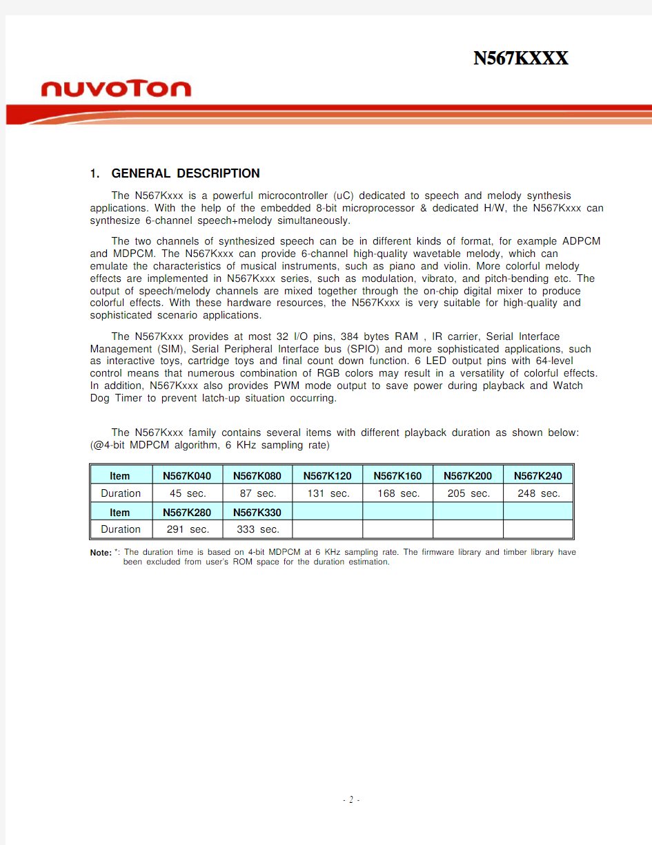
The N567Kxxx family contains several items with different playback duration as shown below: (@4-bit MDPCM algorithm, 6 KHz sampling rate)
Item N567K040 N567K080 N567K120 N567K160 N567K200 N567K240 Duration 45 sec. 87 sec. 131 sec. 168 sec. 205 sec. 248 sec.
Item N567K280 N567K330
Duration 291 sec. 333 sec.
Note: *: The duration time is based on 4-bit MDPCM at 6 KHz sampling rate. The firmware library and timber library have been excluded from user’s ROM space for the duration estimation.
2. FEATURES
?Wide range of operating voltage:
?8 MHz @ 3.0 volt ~ 5.5 volt
? 6 MHz @ 2.4 volt ~ 5.5 volt
?Build in ROSC and system clock setting: 4MHz, 6MHz or 8MHz by Mask Option
? Power management:
? 4 ~ 8 MHz system clocks, with Ring type or crystal type.
?Stop mode for stopping all IC operations
?Provides up to 8 inputs and 24 I/O pins
? N567K040~K200: 24I/O
?N567K240~K330: 8I + 24I/O
?13-bit Current type digital-to-analog converters (DAC) to drive speaker output.
?Direct-drive 12-bit PWM output to save power consumption.
?F/W speech synthesis:
?Multiple format parser that supports
95-bit MDPCM, 4-bit MDPCM, 4-bit ADPCM, 8-bit Log PCM algorithm can be used
?Pitch shippable ADPCM for voice changer application
?Up to 6 speech synthesis1 channels at programmable sample rate
?F/W Melody synthesis:
? 6 melody channels that can emulate characteristics of musical instruments
? Multi-MIDI simultaneous
?Multi-MIDI channels dynamic control
?More MIDI events are supported for colorful melody playback, such as modulation wheel, pitch-bending, pedal, pitch-shift, and vibrato…etc.
?Built-in IR carrier generation circuit for simplifying firmware IR application
?Built-in TimerG1 for general purpose applications
?Harmonized synchronization among MIDI, Speech, LED, and Motor
?Build-in 6 LED outputs (3 pairs) with 64-level control of brightness in N567K240~K330.
?Built-in Watch-Dog Timer (WDT) and Low Voltage Reset (LVR) by mask option
??Provide Serial Interface Management (SIM) to access the external memory in N567K040~K080 and N567K240~K330
? W55Fxx, W551Cxx
? SPI flash
?Build-in Serial Peripheral Interface (SPIO) master/salve mode to communicate with the standard SPI device in N567K240~K330.
? Support PowerScript TM for developing codes in easy way
1 More speech channels are available for 8-bit PCM format in the remaining melody channels. When used as 2-ch MDPCM and 4-ch PCM.
?Full-fledged development system
?Source-level ICE debugger (Assembly & PowerScript TM format)
?Ultra I/O TM tool for event synchronization mechanism
?ICE system with USB port
?User-friendly GUI environment
?Available package form:
?COB is essential
3. PIN DESCRIPTION
PIN NAME
I/O
FUNCTION
RESETB In IC reset input, low active.
OSCIN I Main-clock oscillation input for X’tal mode. Build-in ROSC by mask option.OSCOUT
O
Main-clock oscillation output for X’tal in N567K240~K330 only.
IP0[7:0] In General input port with pull-high selection. Each input pin can be
programmed to generate interrupt request and used to release IC from
STOP mode. It is provided in N567K240~K330 only.
BP0[7:0] I/O
General input/output pins. When used as output pin, it can be open–drain or CMOS type and it can sink 25mA for high-current applications. When used as input pin, there may have a pull-high option and generate interrupt request to release IC from STOP mode. When BP0[7] is used as output pin, it can be the IR transmission carrier for IR applications. BP0[5:0] are used as 6 LED outputs with 64-level control.
BP1[7:0]
I/O General input/output pins. When used as output pin, it can be open–drain or CMOS type. When used as input pin, there may have a pull-high option and generate interrupt request to release IC from STOP mode.
When serial interface management (SIM) is enabled, and set memory type as W55F/W551C, BP1[2:0] are used to be an interface with the
external memory, W55Fxx or W551Cxxx. If set memory to SPI flash,
BP1[3:0] are used to be an interface.
When Serial Peripheral Interface (SPIO) is enabled, BP1[7:4] are shared to communicate with the standard SPI device.
BP2[7:0]
I/O General input/output pins. When used as output pin, it can be open–drain or CMOS type. When used as input pin, there may have a pull-high option
and generate interrupt request to release IC from STOP mode. PWM+/DAC O PWM driver positive output or Current type DAC output PWM- O
PWM driver negative output
VDD Power Positive power supply for uP and peripherals. VSS Power Negative power supply for uP and peripherals. VDDSPK Power Positive power supply for speaker driver.
VSSSPK Power Negative power supply for speaker driver.
VDD_SIM Power Positive power supply for serial interface Management (SIM) BP1[3:0]. VSS_SIM Power Negative power supply for serial interface Management (SIM) BP1[3:0]. VDD_SPI Power Positive power supply for Serial Peripheral Interface (SPIO) BP1[7:4]. VSS_SPI Power Negative power supply for Serial Peripheral Interface (SPIO) BP1[7:4]. VDDOSC Power Positive power supply for oscillator. VSSOSC
Power Negative power supply for oscillator.
4. BLOCK DIAGRAM
BP1[7:0]IP0[7:0]
BP2[7:0]
BP0[7:0] Notes:
1. IP0 is provided in N567K240~N567K330 only.
2. OSCIN/OSCOUT is provided in N567K240~N567K330 only.
5. ELECTRICAL CHARACTERISTICS
5.1 Absolute Maximum Ratings
PARAMETER RATING UNIT
Supply Voltage to Ground Potential
-0.3 to +7.0 V D.C. Voltage on Any Pin to Ground Potential -0.3 to V DD +0.3
V Operating Temperature 0 to +70 °C Storage Temperature
-55 to +150
°C
Note: Exposure to conditions beyond those listed under Absolute Maximum Ratings may adversely affect the life and reliability
of the device.
5.2 D.C. Characteristics
(V DD ?V SS = 4.5 V, F M = 8 MHz, Ta = 25°C, No Load unless otherwise specified)
SPEC.
PARAMETER SYM. TEST CONDITIONS Min. Typ. Max.
UNIT
F SYS = 6 MHz 2.4 - 5.5 V Operating Voltage V DD F SYS = 8 MHz
3.0 - 5.5 V
Operating Current I OP F SYS = 8MHz, normal operation - 8 12 mA Standby Current I SB STOP mode - 1
2
μA Input Low Voltage
V IL
All input pins V SS - 0.3 V DD V Input High Voltage V IH All input pins 0.7 V DD
- V DD
V
Input Current I/O pins, /RESET I IN1 V IN = 0V, pulled-high resistor = 500k ohm -5 -9 -14 μA Input Current I/O pins, /RESET
I IN2 V IN = 0V, pulled-high resistor = 150k ohm -15 -30 -45 μA I OL
V DD = 3V, V OUT = 0.4V 8 12 - mA I OH V DD = 3V, V OUT = 2.6V -4 -6 - mA I OL V DD = 4.5V, V OUT = 1.0V - 25 - mA Output Current (BP0)
I OH V DD = 4.5V, V OUT = 2.6V -
-12
-
mA
Output Low Current I OL V OUT = 0.4V, all output pins except BP0
4 8 - mA Output High Current I OH V OUT = 2.4V, all output pins
except BP0
-4 -6 - mA DAC Full Scale Current I DAC V DD = 4.5V, RL = 100Ω -2.4 -4.0
-3.0 -5.0
-3.6 -6.0
mA
I OL1
+200 - - mA Output Current
PWM+ / PWM-
IOH1
RL= 8 Ohm,
[PWM+]---[RL]---[PWM-]
-200 - - mA
5.3 A.C. Characteristics
(V DD-V SS = 4.5 V, F M= 8 MHz, Ta = 25°C; No Load unless otherwise specified)
SPEC.
CONDITIONS
UNIT
TEST
PARAMETER SYM.
Min. Typ. Max.
ROSC build-in, @3.0~5.5V3973 4096 4218
KHz Main-Clock F M
ROSC build-in, @3.0~5.5V5959 6144 6328
ROSC build-in, @3.0~5.5V7946 8192 8437
ROSC build-in, @2.4~3.6V3973 4096 4218
KHz Main-Clock F M
ROSC build-in, @2.4~3.6V5959 6144 6328
Cycle Time T CYC F SYS = 8 MHz 125 - DC nS
Main-Clock Wake-up
T WSM2^16 clock cycle 8 16 mS Stable Time
RESETB Active Width T RES After F SYS stable 4 - - T CYC
6. TYPICAL APPLICATION CIRCUITS
(a) N567K040~N567K200 DAC Output
Notes:
1. Rosc is built in N567K chip internal. User didn’t need to connect Rosc resistor to OSCIN pin.
2. The Rs value is suggested in 270Ω ~ 1KΩ to limit too large DAC output current flowing into transistor.
3. The capacitor,
4.7uF, shunts between VDD and GND is necessary as power stability. But the value of capacitor is
depend on the application.
4. The above application circuits are for reference only. No warranty for mass production.
(b) N567K040~N567K200 PWM Output
Notes:
1. Rosc is built in N567K chip internal. User didn’t need to connect Rosc resistor to OSCIN pin.
2. The capacitor, 4.7uF, shunts between VDD and GND is necessary as power stability. But the value of capacitor is
depend on the application.
3. The above application circuits are for reference only. No warranty for mass production.
(c) N567K240~N567K330 with SIM application
Notes:
1. Rosc is built in N567K chip internal. User didn’t need to connect Rosc resistor to OSCIN pin.
2. The Rs value is suggested in 270Ω ~ 1KΩ to limit too large DAC output current flowing into transistor.
3. The capacitor,
4.7uF, shunts between VDD and GND is necessary as power stability. But the value of capacitor is
depend on the application.
4. The above application circuits are for reference only. No warranty for mass production..
(d) N567K240~N567K330 with SPIO interface application
Notes:
1. Rosc is built in N567K chip internal. User didn’t need to connect Rosc resistor to OSCIN pin.
2. The capacitor, 4.7uF, shunts between VDD and GND is necessary as power stability. But the value of capacitor is
depend on the application.
3. The above application circuits are for reference only. No warranty for mass production..
7. REVISION HISTORY
VERSION
DATE
REASONS FOR CHANGE
A0
June 2009
Preliminary release.
A1 July 2009
? SIM is provided in N567K040~K080.
? PWM speaker output is provided in N567K040~K080.
A2 August 2009 ? Add VDDOSC and VSSOSC in the pin description
? Remove TEST pad in the pin description
? Modify N567K240~K330 application circuit
A3 August 2009 ? Modify Frequency deviation in 5.3 A.C. Characteristics.
A4 September 2009
? Modify Main Clock and Frequency deviation condition in 5.3 A.C.Characteristics. A5 October 2009 ? Remove LVD function in 2 Features
A6 November 2009
? Revise frequency deviation value of 2.4~3.6V in section 5.3 A.C. Characteristics.
Important Notice
Nuvoton products are not designed, intended, authorized or warranted for use as components in systems or equipment intended for surgical implantation, atomic energy control instruments, airplane or spaceship instruments, transportation instruments, traffic signal instruments, combustion control instruments, or for other applications intended to support or sustain life. Further more, Nuvoton products are not intended for applications wherein failure of Nuvoton products could result or lead to a situation wherein personal injury, death or severe property or environmental damage could occur.
Nuvoton customers using or selling these products for use in such applications do so at their own risk and agree to fully indemnify Nuvoton for any damages resulting from such improper use or sales.