低压芯片FP5202升压IC

General Description
The FP5202 is a boost topology switching regulator for wide operating voltage applications. It provides built-in gate driver pin for driving an external N-MOSFET. The internal compensation network minimizes external component counts, and the non-inverting input of error amplifier connects to a 0.6V precision reference voltage. The FP5202 has internal soft start and programmable over current protection set by external resistance.
The FP5202 is available in the small footprint SOT23-6L package to fit in space-saving PCB layout for miscellaneous application fields.
Features
Wide Supply Voltage Operating Range: 2.4 to 5.5V Precision Feedback Reference Voltage: 0.6V (±2%) Shutdown Current: <1μA
Internal Fixed PWM frequency: 550KHz Internal Soft Start Function :7ms (SS) Over Current Protection Function (OCP) Over Voltage Protection Package: SOT23-6L
Duty Cycle: PWM/PFM Switching Control Circuit (15%~90%)
Applications
Chargers LCD Displays Digital Cameras Handheld Devices Portable Products
Typical Application Circuit
This datasheet contains new product information. Feeling Technology reserves the rights to modify the product specification without notice. No liability is assumed as a result of the use of this product. No rights under any patent accompany the sales of the product.
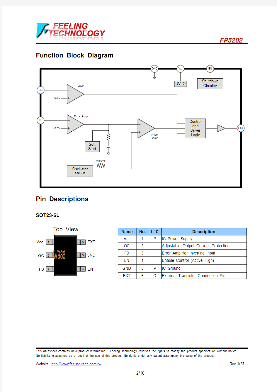
Function Block Diagram
Pin Descriptions
SOT23-6L
V CC EN
OC FB
Top View
GND EXT
This datasheet contains new product information. Feeling Technology reserves the rights to modify the product specification without notice. No liability is assumed as a result of the use of this product. No rights under any patent accompany the sales of the product.
Marking Information
SOT23-6L
Lot Number Part Number Code
Year
Lot Number : Wafer lot number ’s last two digits
For Example: 132386TB 86 Year : Production year ’s last digit Part Number Code : Part number identification code for this product. It should be always “AV ”.
This datasheet contains new product information. Feeling Technology reserves the rights to modify the product specification without notice. No liability is assumed as a result of the use of this product. No rights under any patent accompany the sales of the product.
IR Re-flow Soldering Curve
This datasheet contains new product information. Feeling Technology reserves the rights to modify the product specification without notice. No liability is assumed as a result of the use of this product. No rights under any patent accompany the sales of the product.
This datasheet contains new product information. Feeling Technology reserves the rights to modify the product specification without notice. No liability is assumed as a result of the use of this product. No rights under any patent accompany the sales of the product.
Function Description
Operation
The FP5202 is a voltage mode boost controller. It operates with pulse width modulation (PWM) at fixed 550kHz switching frequency. An internal resistive divider provides 0.6V reference for the error amplifier. The FP5202 changes to PFM mode when output is light load. It can increase efficiency, but PFM mode also increases output voltage ripple.
Soft Start Function
Soft start circuitry is integrated into FP5202 to avoid inrush current during power on. After the IC is enabled, the output of error amplifier is clamped by the internal soft-start function, which causes PWM pulse width increasing slowly and thus reducing input surge current.
Over Current Protection
The FP5202 provides an output current limit protection function. The circuit is shown in Figure 1. The output current limiting will be activated when the OC pin voltage is higher than 0.1V.
To set the over current trip point, follow below equation:
Roc 1.0=
I OCP
Figure1. OC pin circuit
Shutdown Function
Drive Enable pin to ground to shut down the FP5202. Shutdown mode forces to turn off all internal circuitry, and reduces the Vcc supply current to 0.1μA (typ). The Enable pin rising threshold is 0.96V (typ). Before any operation begins, the voltage at Enable pin must exceed 0.96V (typ).
This datasheet contains new product information. Feeling Technology reserves the rights to modify the product specification without notice.
No liability is assumed as a result of the use of this product. No rights under any patent accompany the sales of the product.
Application Information
Inductor Selection
Inductance value is decided based on different condition. 3.3uH to 4.7μH inductance value is recommended for general application circuit. There are three important inductor specifications, DC resistance, saturation current and core loss. Low DC resistance has better power efficiency.
Capacitor Selection
The output capacitor is required to maintain the DC voltage during switching. Low ESR capacitors are preferred to reduce the output voltage ripple. Ceramic capacitor of X5R and X7R are recommended, which have low equivalent series resistance (ESR) and wider operation temperature range.
Diode Selection
Schottky diodes with fast recovery times and low forward voltages are recommended. Ensure the diode average and peak current rating exceed the average output current and peak inductor current. In addition, the diode’s reverse breakdown voltage must exceed the output voltage.
Output Voltage Programming
The output voltage is set by a resistive voltage divider from the output voltage to FB. The output voltage is:
??
? ??
+=2R 1R 1V 6.0V OUT
This datasheet contains new product information. Feeling Technology reserves the rights to modify the product specification without notice. No liability is assumed as a result of the use of this product. No rights under any patent accompany the sales of the product.
Layout Considerations
1.
The power traces, consisting of the GND trace, the MOS drain trace and the V CC trace should be kept short, direct and wide. 2.
Layout switching node MOS drain, inductor and diode connection traces wide and short to reduce EMI. 3.
Place C IN nearby V CC pin as closely as possible to maintain input voltage steady and filter out the pulsing input current. 4. The resistive divider R1 and R2 must be connected to FB pin directly and as closely as possible. 5. FB is a sensitive node. Please keep it away from switching node, MOS drain.
6.
The GND of the IC, C IN and C OUT should be connected close and together directly to a ground plane. 7. OC pin is a sensitive node. Roc must be connected to IC GND pin directly as closely as possible. 8. OC pin is not connected (floating) when OC function is disabled. Don’t connect to GND directly. 9.
The output capacitor C2 and C3 should be connected close and together directly to the source of MOS.
Suggested Layout
This datasheet contains new product information. Feeling Technology reserves the rights to modify the product specification without notice. No liability is assumed as a result of the use of this product. No rights under any patent accompany the sales of the product.
Application Information
L1 3.3μH
L1 3.3μH
Note:
1. C1 and C3 choose ceramic capacitor of X5R or X7R.
2.
R3 and C5 are added for reducing EMI (Electromagnetic Interference).
This datasheet contains new product information. Feeling Technology reserves the rights to modify the product specification without notice. No liability is assumed as a result of the use of this product. No rights under any patent accompany the sales of the product.
Package Outline
SOT23-6L
Unit: mm
Note:
1. Package dimensions are in compliance with JEDEC outline: MO-178 AB.
2. Dimension “D” does not include molding flash , protrusions or gate burrs.
3. Dimension “E1” does not include inter -lead flash or protrusions.
ZCC9430 DC-DC同步升压芯片-内置MOS
ZCC9430同步升压芯片 一、产品综述 ZCC9430芯片是一款具有600KHz的自动调节频率、高效率、宽输入范围的电流模式升压(BOOST)芯片,且具有高效率同步升压功能和可调限流功能。该电源芯片内部全集成低内阻功率MOSFET,可以实现大功率输出的同时,大大简化了外部电路设计,同时实现低功耗,高效率电源开关。用户可灵活地通过外部补偿建立动态环路,获得在所有条件下最优瞬态性能。 ZCC9430芯片还包括欠压锁存,过流保护和过温保护,以防止在输出过载时产生损害。二、产品特点 ? 完全符合Intel Thunderbolt Power Spec. ? 输入限流电阻,灵活设置最大输出功率? 输入最大电流可达8A ? 自动调频,最大限度降低功耗 ? 增强PWM模式的快速瞬态响应 ? 3.0 V-30V宽输入范围 ? 输出电压:5V To 30V ? 芯片停止工作时电流< 1μA 三、产品应用 ? Thunderbolt 接口 ? 笔记本电脑和平板电脑 ? 热插拔电源管理 ? 通信供应电源 四、典型应用电路
ZCC9430同步升压芯片 五、采用QFN20 5mm*5mm封装 绝对最大额定参数(1): SW, OUT ....... ..............–0.5V to +35V IN, SENSE .... ................–0.5V to +35V BST, SDR ....... ........–0.5V to Vsw+5V 其他管脚....... ...............–0.3V to +5V EN 偏置电流……...... ..........… 0.5mA 结温度................ .... .................. 150°C 存储温度. ....... .......... -65°C to +150°C 额定功耗 (TA......=+25°C)....2.6W(2) 推荐的操作条件(3) 电源电压VIN..............3.0V to 30V 输出电压 VOUT........ 5V to 30V EN 偏置电流……0mA to 0.3mA 操作临界温度. ....-40°C to +125°C 注: 1)超过这些额定参数可能损坏设备。 2)最大允许功耗是一个关于最大临界温度T J(MAX),过热保护电阻θJA,环境温度T A的函数。在任何环境温度下的最大允许额定功耗计算公式为P D(MAX)=(T J(MAX)-T A)/θJA。超过了最大允许功耗将导致过温,导致产生过温保护。内部过温保护电路保护芯片免受永久性的损害。 3)芯片不能保证其在操作条件以外运行。
LED升压、升降压的驱动恒流IC推荐一
LED升压、升降压的驱动恒流IC推荐一 宝剑锋从磨砺出,梅花香自苦寒来;此句是中国流传下来的一句古训,喻为如果想要取得成绩,获取成就,就要能吃苦,勤于锻炼,这样才能靠自己的努力赢得胜利。各个行业皆是如此。在电源网论坛里,就存在 这样一些人,他们时常能DIY出被网友们称之为的经典设计,出于大家能够共同学习的目的,小编抓住了难得的机会,整理了这些经典帖,供分享学习。 今天小编与您分享的同样是来自文子的精华帖。--------小编语。 在LED产品设计中经常会用到升压或升降压线路设计,变压器可以升压设计但是效率较低,未来低压还是线路器件直接升压转换为主,效率高、体积小巧可靠。市场主要升压LED驱动恒流IC应用在手持式设备、蓄电池中蓄产品中。比如干电池、镍氢电池升压;锂电池升降压;汽车蓄电池主灯升压;户外离网照明和 灯带式方式解决级联供电压差问题等方面。本文将主要介绍升压和升降压驱动IC及设计中需要注意的问题。TI 美国德州仪器公司TPS61165 LED升压转换器 具备40V、1.2A集成开关的高亮度LED驱动器,该产品可驱动多达三个串联1W LED。新型TPS61165器件具备优异的高性能特性以及3V~18V的宽泛输入电压范围,使设计人员能够在采用单节电池供电的应用或9V/12V总线负载点设计中高效管理多个高功率LED。 TPS61165通过数字单线接口或脉宽调制(PWM)信号来控制LED的亮度。数字接口可对内部寄存器进行编程,以将LED电流设置为32个对数步长值之一。此外,该转换器还具有多种内置保护特性,如LED开路保护、软启动、过流限制以及过温保护等。除了能够驱动照明LED之外,TPS61165还可驱动背光LED,支持宽度达9英寸的多媒体显示屏,从而满足超级移动PC、LCD 电子相框、工业激光二极管或医疗以及 工业照明等应用的需求。
升压恒压IC驱动IC方案
特点 n 5V 到40V 宽输入电压范围 n 1.25V 输出电压采样电压 n SW 内置过压保护功能 n 固定220KHz 开关频率 n 最大5A 开关电流 n 94%以上转换效率 n EN 脚TTL 关断功能 n 出色的线性与负载调整率 n 内置功率MOS n 内置频率补偿功能 n 内置软启动功能 n 内置热关断功能 n 内置电流限制功能 n TO263-5L 封装 应用 n EPC/笔记本车载适配器 n 升压、升降压转换 n 手持式设备供电 XL6019是一款专为升压、升降压设计的单片集成电路,可工作在DC5V 到40V 输入电压范围,低纹波,内置功率MOS 。XL6019内置固定频率振荡器与频率补偿电路,简化了电路设计。 PWM 控制环路可以调节占空比从0~90%之间线性变化。内置过电流保护功能与EN 脚逻辑电平关断功能。 图1. XL6019封装
220KHz 60V 5A开关电流升压/升降压型DC-DC转换器XL6019 引脚配置 图2. XL6019引脚配置 表1.引脚说明 引脚号引脚名描述 1 GND 接地引脚。 2 EN 使能引脚,低电平关机,高电平工作,悬空时为高电平。 3 SW 功率开关输出引脚,SW是输出功率的开关节点。 4 VIN 电源输入引脚,支持5V到40V DC范围电压输入,需要在VIN 与GND之间并联电解电容以消除噪声。 5 FB 输出电压采样引脚,FB参考电压为1.25V。
220KHz 60V 5A 开关电流升压/ 升降压型DC-DC 转换器 XL6019 方框图 图3. XL6019方框图 典型应用 VOUT=1.25*(1+R2/R1) L1 47uH/5A 图4. XL6019系统参数测量电路
XC9119 DCDC升压芯片
XC9119D10A Series 1MHz, PWM Controlled, Step-Up DC/DC Converter, Ceramic Capacitor Compatible ETR0408_008 ■GENERAL DESCRIPTION The XC9119D10A series is 1MHz, PWM controlled step-up DC/DC converter, designed to allow the use of ceramic capacitors. With a built-in 2.0Ω switching transistor, the XC9119D10A series can easily provide a step-up operation by using only a coil, a diode, a capacitor, and a resistor, connected externally. Since output voltage up to 19.5V (Maximum Lx operating voltage: 20V) can be derived with reference voltage supply of 1.0V (±2.0%) and external components, the series can easily supply high voltage for various general-purpose power supplies, LCD panels and organic EL displays. With a high switching frequency of 1.0MHz, a low profile and small board area solution can be achieved using a chip coil and an ultra small ceramic output capacitor. With the current limit function (400mA (TYP .): V DD =3.6V), a peak current, which flows through built-in driver transistors can be limited. Soft-start time can be adjusted by external resistors and capacitors. The stand-by function enables the output to be turned off (CE ’L’), that is, the supply current will be less than 1.0?A. ■TYPICAL APPLICATION CIRCUIT ■APPLICATIONS ●Organic electroluminescence display (OELD)●Power supplies for LCDs ●Multi-function power supplies ■FEATURES Operating Voltage Range : 2.5V ~ 6.0V Output Voltage Range : Up to 19.5V externally set-up : Reference voltage 1.0V +2.0% Oscillation Freq uency : 1.0MHz ±20% ON Resistance : 2.0Ω (V DD =3.6V, V DS=0.4V) Efficiency : 86% (V OUT =15V, V DD =3.6V, I OUT =10mA) Control : PWM control Stand-by function : I STB =1.0?A (MAX.) Load Capacitor : Low ESR ceramic capacitor Ultra Small Packages : SOT-25, USP-6C Lx Limit Current : 400mA (V DD =3.6V) ■TYPICAL PERFORMANCE CHARACTERISTICS ○Efficiency vs. Output Current 1020304050607080901000.1 1 101001000 Output Current: I OUT (mA) E f f i c i e n c y : E F F I (%) XC9119D10A 1/18
升压芯片-TPS系列
10Low-power DC/DC converter selection guides Page 7TPS6110x,Dual output DC/DC converter with integrated LDO offers complete power supply solution in one device Page 8TPS6220x, 97% efficient step-down converter in SOT-23TPS62202GND Vin EN SW FB 10 μH 2.5 V . . . 6.0 V 1.8 V/300 mA 100.0090.0080.0070.0060.0050.0040.0030.0020.0010.000.00 3.60.010.11101001000Iout/mA TPS62202 efficiency vs. Iout U p d a te d 2Q '02 R E A L W O R L D S I G N A L P R O C E S S I N G TM Actual Size (3.0 mm x 3.0 mm)SOT -23 package QFN/MLP-24 package 10 μH TPS61106 3.3 V LBO1LBO2PGOOD 1.5 V >250 mA >120 mA SWN SWN LBI SKIPEN ADEN EN ENPB ENLDO GND PGND PGOOD LB02LB01LDOSENSE LDOOUT LDOIN VOUT 0.8 V . . . 3.3 V Battery Order your free copy of the UPDATED 'Power Management Selection Guide' Actual Size (4.0 mm x 4.0 mm)?
HX3141 DC-DC升压IC
HX1001 T i n y P a c k a g e,H i g h E f f i c i e n c y,S t e p-u p F e a t u r e s Input Voltage Range: 1.1V~5.5V Internal MOSFET with high switch current up to 3A 90% Efficiency Up to 450kHz Switching Frequency SOT-23-6L Package A p p l i c a t i o n s PDA DSC LCD Panel RF-Tags MP3 Portable Instruments Wireless Equipments D e s c r i p t i o n The HX3141 is a compact, high efficiency, and low voltage step-up DC/DC converter including an error amplifier, ramp generator, comparator, switch pass element and driver in which providing a stable and high efficient operation over a wide range of load currents. It operates in stable waveforms without external compensation. The high switching rate minimized the size of external components. Besides, the low quiescent current together with high efficiency maintains long battery lifetime. The output voltage is set with two external resistors. The HX3141 is available in the industry standard SOT-23-6L power packages.
带输出关断的 20V,14A 全集成同步升压转换器
带输出关断的20V,14A 全集成同步升压转换器 HT7178是一款高功率、全集成升压转换器,带有负载关断功能的栅极驱动,集成16mΩ功率开关管和16mΩ同步整流管,为便携式系统提供gao效的小尺寸解决方案。HT7178具有2.7V至20V宽输入电压范围,可为采用单节或两节锂电池,或12V铅酸电池的应用提供支持。该器件具备14A开关电流能力,并且能够提供高达20V的输出电压。HT7178采用自适应恒定关断时间峰值电流控制拓扑结构来调节输出电压。在中等到重负载条件下,HT7178 工作在PWM 模式。在轻负载条件下,该器件可通过MODE引脚选择下列两种工作模式之一。一种是可提gao效率的PFM模式;另一种是可避免因开关频率较低而引发应用问题的强制PWM模式。PWM模式下,HT7178的开关频率可通过外部电阻调节,支持200kHz至1.4MHz的范围。HT7178还支持可编程的软启动,以及可调节的开关峰值电流限制。另外,HT7178集成了输出关断功能的栅极驱动,在SD状态,可完全断开输入电源。此外,该器件还提供有22V输出过压保护、逐周期过流保护和热关断保护。 加扣1165357467 ?特点 ?输入电压范围V PIN :2.7V-20V ?输出电压范围V OUT :4.5V-20V ?可编程峰值电流:14A ?高转换效率: 95% (V PIN = 7.2V, V OUT =16V, I OUT =3A) 94% (V PIN = 12V, V OUT =18V, I OUT =4A) 90% (V PIN = 3.3, V OUT =9V, I OUT =3A) ?轻载条件下两种调制方式:脉频调制(PFM)和
MC3406芯片DC_DC转换升压电路
电子技术课程设计报告 设计课题:MC3406芯片DC/DC转换升压电路 专业班级: 学生姓名: 指导教师: 设计时间:2011.10.15-2011.12.15 目录 1 设计任务与要求 (3) 2 集成稳压电源和开关电源的区别 (3)
2.1 集成稳压器的组成 (3) 2.2 开关电源的组成 (4) 3 开关电源的分类 (5) 4 常见开关电源的介绍 (6) 4.1基本电路 (6) 4.2 单端反激式开关电源 (7) 4.3单端正激式开关电源 (7) 4.4自激式开关稳压电源 (8) 4.5 推挽式开关电源 (9) 4.6 降压式开关电源 (9) 4.7 升压式开关电源 (10) 4.8 反转式开关电源 (10) 5设计升压开关电源并计算参数 (11) 5.1 MC34063的介绍 (11) 5.2MC34063组成的升压电路原理 (12) 5.3电路的参数设计计算 (14) 6 性能测试结果分析 (17) 7.结论与心得 (18) 8.参考文献 (18) 9.附录 (19) 基于MC34063的稳压电源设计 一、设计任务与要求 1.掌握PCB制板技术、焊接技术、电路检测以及集成电路的使用方法。
2.掌握mc34063的非隔离开关电源的设计、组装与调试方法。 3.研究开关电源的实现方法,并按照设计指标要求进行电路的设计与仿真。具体要求如下: ①分析、掌握该课题总体方案,广泛阅读相关技术资料,并提出见解。 ②掌握开关电源的工作原理。 ③设计硬件系统并进行仿真,掌握系统调试方法,使系统达到设计要求。主要技术指标 直流输入电压:5~12V; 输出电压:28V; 输出电流:0.3A; 效率:≥90%。 二、集成稳压电源和开关电源的区别: (1)、集成稳压器的组成 电路内部包括了串联型直流稳压电路的各个组成部分,另外加上保电路和启动电路。 1. 调整管 在W7800系列三端集成稳压电路中,调整管为由两个三极管组成的复合管。这种结构要求放大电路用较小的电流即可驱动调整管发射极回路中较大的输出电流,而且提高了调整管的输入电阻。 2.放大电路 在W7800系列三端集成稳压电路中,放大管也是复合管,电路组态为共射接法,并采用有源负载,可以获得较高的电压放大倍数。
手电筒IC升压方案
概述 QX2303系列产品是一种高效率、低纹波、工作频率高的PFM升压DC-DC变换器。 QX2303系列产品仅需要四个元器,就可完成将低输入的电池电压变换升压到所需的工作电压,非常适合于便携式1~4 节普通电池应 用的场合。 电路采用了高性能、低功耗的参考电压电 路结构,同时在生产中引入修正技术,保证了输出电压的高输出精度及低温度漂移。 QX2303可提供SOT-23-3, SOT-23-5, SOT-89封装形式,SOT23-5封装内置EN使能端,可控制变换器的工作状态,可使它处于关断省电状态,功耗降至最小。 订货信息 特性 ?最高工作频率:300KHz ?输出电压:2.0V~5.0V(步进0.1V) ?低起动电压:0.8V(1mA) ?输出精度:优于±2.5% ?最高效率:87% ?输出电流:大于300mA(Vi=2.5V,Vo=3.3V)?低纹波,低噪声 应用范围 1~3个干电池的电子设备,如:电子词典、数码相机、LED手电筒、LED灯、血压计、MP3、遥控玩具、无线耳机、无线鼠标键盘、医疗器械、防丢器、汽车防盗器、充电器、VCR、PDA 等手持电子设备
典型应用电路图
方框图
管脚定义 封装型式和管脚号 符号 QX2303 LXXT SOT-23-3 QX2303 LXXF SOT-23-5 QX2303 LXXE SOT-89 说明 LX 2 5 3 开关脚 VOUT 3 2 2 输出电压 EN - 1 - 使能端 GND 1 4 1 地 EXT 3 扩展脚
最大额定参数值 参数符号说明典型值单位Vmax 供给U OUT和V LX端的最大电压值 8 V 电压 Vmin-max 在EN端的电压范围 -0.3-VOUT+0.3V 电流 ILXmax LX端最大电流 1000 mA Psot-23-3 SOT-23-3封装最大电流功耗 0.25 W Psot-23-5 SOT-23-5封装最大电源功耗 0.25 W 电源功耗 Psot-89 SOT-89封装最大电源功耗 0.5 W Tmin-max 工作温度范围 -20-85 o C 温度 Tstorage 存储温度范围 -40-165 o C ESD VESD 人体静电耐压值 2000 V 电气特性 参数符号测试条件最小值典型值最大值单位输出电压精度 △VOUT -2.5 2.5 % 最大输入电压VIN MAX 0.7 VOUT V 起动电压V START ILOAD=1mA, VIN:0→ 2V 1.2 V 保持电压V HOLD ILOAD=1mA, VIN:2→ 0V 0.9 V 最大振荡频率F MAX 200 300 350 KHz 振荡信号占空比DC OSC 75 80 85 % 效率η84 88 % 限流I LIMIT 600 800 1000 mA VIN=1.8V VOUT=3.0V 11.8 uA 无负载状态下输入电流IIN0 VIN=1.8V VOUT=5.0V 7 uA 待机(省电)状态输入电流IINQ No load, EN=“low” 1 uA EN “高”电压值 0.4*VOUT V EN “低”电压值0.2 V EN “高” 输入电流0.1 uA -0.1 uA
升压IC内置MOS管高性价比方案
n 5V 到40V 宽输入电压范围 n 0.22V 输出电流采样电压 n 输出可驱动2~10串1W LED n 固定400KHz 开关频率 n 最大2A 开关电流 n SW 内置过压保护功能 n 93%以上转换效率 n EN 脚TTL 关断功能 n 出色的线性与负载调整率 n 内置功率MOS n 内置频率补偿功能 n 内置软启动功能 n 内置热关断功能 n 内置电流限制功能 n SOP-8L 封装 应用 n 升压恒流驱动 n 显示器LED 背光 n 通用LED 照明 图1. XL6013封装 器,可工作在DC5V 到40V 输入电压范围,低纹波,内置功率MOS 。XL6013内置固定频率振荡器与频率补偿电路,简化了电路设计。 当输入电压大于或等于12V 时,XL6013可驱动5至10串1W LED 。 PWM 控制环路可以调节占空比从0~90%之间线性变化。内置过电流保护功能与EN 脚逻辑电平关断功能。内部补偿模块可以减少外围元器件数量。
400KHz 60V 2A 开关电流升压型LED 恒流驱动器 XL6013 引脚配置 SW EN FB VIN NC SW GND GND 图2. XL6013引脚配置 表1.引脚说明 引脚号 引脚名 描述 1 EN 使能引脚,低电平关机,高电平工作,悬空时为高电平。 2 VIN 电源输入引脚,支持5V 到40V DC 范围电压输入,需要在VIN 与GND 之间并联电解电容以消除噪声。 3 FB 输出电流采样引脚,FB 参考电压为0.22V 。 4 NC 无连接。 5,6 SW 功率开关输出引脚,SW 是输出功率的开关节点。 7,8 GND 接地引脚。
SY7208互换的升压型DC-DC转换器MXT7515
2.3V to 6V input voltage Rangel Efficiency up to 96% 26V Boost converter with 2.8A switch current 1.2Mhz fixed Switching Frequency Integrated soft-start Thermal Shutdown Under voltage Lockout SOT23-6 Package is a high frequency, high efficien cy DC to DC converter with an integrated 2.8A, 0.1Ω power switch capable of providing an output voltage up to 26V.The fixed 1.2MHz allows the use of small external inducti ons and capacitors and provides fast transien t response. It integrates Soft start, Comp. On ly need few components outside. Handheld Devices GPS Receiver Digital Still Camera Portable Applications DSL Modem PCMCIA Card TFT LCD Bias Supply Figure 1 Typical Application Circuit 5 1 2 3 6 IN EN GND SW FB NC 4 2.3V to 6V Cbv 16V 1μFMXT75151.2MHZ,26V Step-up DC/DC Converter Features GENERAL DESCRIPTION APPLICATIONS MXT7515The
DC-DC升压(BOOST)电路原理
DC-DC升压(BOOST)电路原理 BOOST升压电路中: 电感的作用:是将电能和磁场能相互转换的能量转换器件,当MOS开关管闭合后,电感将电能转换为磁场能储存起来,当MOS断开后电感将储存的磁场能转换为电场能,且这个能量在和输入电源电压叠加后通过二极管和电容的滤波后得到平滑的直流电压提供给负载,由于这个电压是输入电源电压和电感的磁砀能转换为电能的叠加后形成的,所以输出电压高于输入电压,既升压过程的完成; 肖特基二极管主要起隔离作用,即在MOS开关管闭合时,肖特基二极管的正极电压比负极电压低,此时二极管反偏截止,使此电感的储能过程不影响输出端电容对负载的正常供电;因在MOS管断开时,两种叠加后的能量通过二极向负载供电,此时二极管正向导通,要求其正向压降越小越好,尽量使更多的能量供给到负载端!!
在图2所示的实际电路中,带集成功率MOSFET的IC代替了机械开关,MOSFET的开、关由脉宽调制(PWM)电路控制。输出电压始终由PWM占空比决定,占空比为50%时,输出电压为输入电压的两倍。将电压提高一倍会使输入电流大小达到输出电流的两倍,对实际的有损耗电路,输入电流还要稍高。 电感值如何影响电感型升压转换器的性能? 因为电感值影响输入和输出纹波电压和电流,所以电感的选择是感性电压转换器设计的关键。等效串联电阻值低的电感,其功率转换效率最佳。要对电感饱和电流额定值进行选择,使其大于电路的稳态电感电流峰值。 电感型升压转换器IC电路输出二极管选择的原则是什么? 升压转换器要选快速肖特基整流二极管。与普通二极管相比,肖特基二极管正向压降小,使其功耗低并且效率高。肖特基二极管平均电流额定值应大于电路最大输出电压. 怎样选择电感型升压转换器IC电路的输入电容? 升压调节器的输入为三角形电压波形,因此要求输入电容必须减小输入纹波和噪声。纹波的幅度与输入电容值的大小成反比,也就是说,电容容量越大,纹波越小。如果转换器负载变化很小,并且输出电流小,使用小容量输入电容也很安全。如果转换器输入与源输出相差很小,也可选小体积电容。如果要求电路对输入电压源纹波干扰很小,就可能需要大容量电容,并(或)减小等效串联电阻(ESR)。
大电流升压恒压IC方案
400KHz 60V 3A Switching Current Boost / Buck-Boost / Inverting DC/DC Converter Features n Wide 3.6V to 32V Input Voltage Range n Positive or Negative Output Voltage Programming with a Single Feedback Pin n Current Mode Control Provides Excellent Transient Response n 1.25V reference adjustable version n Fixed 400KHz Switching Frequency n Maximum 3A Switching Current n SW PIN Built in Over Voltage Protection n Excellent line and load regulation n EN PIN TTL shutdown capability n Internal Optimize Power MOSFET n High efficiency up to 92% n Built in Frequency Compensation n Built in Soft-Start Function n Built in Thermal Shutdown Function n Built in Current Limit Function n Available in TO252-5L package Applications n Automotive and Industrial Boost / Buck-Boost / Inverting Converters n Portable Electronic Equipment General Description The XL6008 regulator is a wide input range, current mode, DC/DC converter which is capable of generating either positive or negative output voltages. It can be configured as either a boost, flyback, SEPIC or inverting converter. The XL6008 built in N-channel power MOSFET and fixed frequency oscillator, current-mode architecture results in stable operation over a wide range of supply and output voltages. The XL6008 regulator is special design for portable electronic equipment. Figure1. Package Type of XL6008
200款Prius的升压转换器
Development of Hybrid Electric Drive System Using a Boost Converter Masaki Okamura Eiji Sato Shoichi Sasaki TOYOTA MOTOR CORPORATION 1, Toyota-cho, Toyota, Aichi, 471-8572, Japan Phone/ Fax : +81-565-72-9071/9147 Abstract Toyota introduced a new generation of hybrid vehicle to the market in September of 2003. The new Prius, equipped with a new Toyota-developed inverter system, is capable of outputting more power than the conventional systems. One of the strong points of this new system is that a Boost Converter has been placed between the inverter and the battery. The Boost Converter is capable of raising the voltage from the battery, enabling the inverter to drive a high power output motor. The Toyota Hybrid System (THS), consists of a high power motor, generator, and a battery of relatively lower power. When the Boost Converter was adopted in the THS, it was possible to keep bulk and cost of the additional unit in the system to a minimum, by letting the Boost Converter function to the same power level as the battery. The control system of the Boost Converter consists simply of a PI controller. By using existing sensors and microprocessors, it was possible to develop a new system at no additional costs. The Boost Converter’s control system achieves high efficiency by optimizing its output voltage according to the relative state of the motor and the generator. Toyota was able to achieve a 50% improvement in the motor power output with the new Boost Converter, while keeping a similar complexity of the conventional system. As of now, Toyota plans to spread the development to other new hybrid vehicles.__ Keywords: Hybrid, Electric Drive, Converter, Inverter, Control System Figure1: TOYOTA NEW PRIUS
升压芯片之RT9212
DS9212-05 March 2007 https://www.wendangku.net/doc/a43929518.html, Dual 5V Synchronous Buck PWM DC-DC and Linear Power Controller Features z Operating with Single 5V Supply Voltage z Drives All Low Cost N-MOSFETs z Voltage Mode PWM Control z 300kHz Fixed Frequency Oscillator z Fast Transient Response :Full 0% to 100% Duty Ratio z Internal Soft-Start z Adaptive Non-Overlapping Gate Driver z Over-Current Fault Monitor on V CC , No Current Sense Resistor Required z RoHS Compliant and 100% Lead (Pb)-Free Applications z Graph Card z Motherboard, Desktop Servers z IA Equipments z Telecomm Equipments z High Power DC-DC Regulators Pin Configurations Ordering Information General Description The RT9212 is a 3-in-one power controller delivers high efficiency and tight regulation from two voltage regulating synchronous buck PWM DC-DC and one linear power controllers. The RT9212 can control two independent output voltages adjustment in range of 0.8V to 4.0V with 180 degrees channel to channel phase operation to reduce input ripple.In dual power supply application the RT9212 monitors the output voltage of both Channel 1 and Channel 2. An independent PGOOD (power good) signal is asserted for each channel after the soft-start sequence has completed,and the output voltage is within ±15% of the set point. The linear controller drives an external transistor to provide an adjustable output voltage. Built-in over-voltage protection prevents the output from going above 137.5% of the set point by holding the lower MOSFET on and the upper MOSFET off. Adjustable over-current protection (OCP) monitors the voltage drop across the R DS(ON) of the upper MOSFET for each synchronous buck PWM DC-DC controller individually. (TOP VIEW) UGATE1BOOT1PHASE1 NC OCSET2/SD OCSET1/SD PVCC1 PGND1FB1COMP1 FB2PGOOD NC LGATE1FBL NC GNDA VCC DRV PHASE2BOOT2PGND2 LGATE2UGATE2 TSSOP-24 Note : RichTek Pb-free and Green products are : `RoHS compliant and compatible with the current require- ments of IPC/JEDEC J-STD-020. `Suitable for use in SnPb or Pb-free soldering processes.`100% matte tin (Sn) plating. RT9212 P : Pb Free with Commercial Standard G : Green (Halogen Free with Commer- cial Standard)
输出高压的小型升压转换器
输出高压的小型升压转换器 输出高压的小型升压转换器 有许多器件需要高压电源,如雪崩二极管(APD)的偏置电源、压电传感器(PZT)、真空荧光屏(VFD)以及微机电系统(MEMS)等。本应用笔记介绍了三种从低输入电压产生高压输出的结构(图1a、图1b和图1c)。下面将针对其功率密度和电路尺寸,分别讨论这些结构的优点和缺点。在应用笔记结尾部分,列举了一些实验数据,以对比基于变压器和基于电感的解决方案。 图1a-1c. 从低输入电压产生高压输出的高压DC-DC转换器的三种结构 在许多APD应用(75V)中,高压偏置电源要求从3V电源产生。这种需求将面临以下难点: 高压MOSFET在3V低压栅极驱动下无法工作。 高压MOSFET较大的漏源电容需要消耗电感中的能量,将其漏极电压提升至输出电压。导致的能损会高达1/2 fswitch×CDSVOUT 2。 高压MOSFET比低电压型号的体积更大、价格更高。在开关电源IC中,很少具有内置的高压功率MOSFET。 极端情况下的占空比会导致过短的关断时间或很低的开关频率。较低的开关频率又会造成更高的纹波,并需要较大的磁性元件。 图1c的电路通过采用一个自耦变压器,解决了上述难题。由于MOSFET上的峰值电压降低了,从而能够采用MAX1605内部的28V MOSFET。整个电路(比8引脚的DIP封装还小)能 够装配在一块6mm x 8.5mm的双面板上(图2)。 图2. 采用MAX1605,该6mm x 8.5mm的DC-DC转换器将2.5V升压至75V。顶层和底层的电路布局如图所示。
工作原理 工作原理 将标准的升压和回扫DC-DC转换器结合起来,就构成了图1c所示的混合电路。这种组合结构将次级绕组的回扫电压叠加到输入电压和初级绕组的回扫电压之上(标准的回扫转换器仅利用了次级端产生的回扫电压)。与标准的升压转换器相比,这种结构通过限制LX端电压,利用低压MOSFET产生了较高的输出电压。 变压器提供了下列优点: 更高的输出电压 较小的工作占空比 MOSFET上承受的电压更低 当变压器工作在非连续模式下,且MOSFET的峰值电流恒定时,还具有以下优点: 更高的开关频率产生的输出纹波更小 更高的纹波频率 较小的磁性元件 MAX1605以及其它许多升压转换器都能够采用这种结构。最高输出电压受限于变压器的匝数比、变压器和二极管的额定电压、MOSFET的额定电压和漏极电容、以及二极管的反向恢复时间。 标准升压电路 标准升压电路 标准的升压转换器如图1a所示。当MOSFET闭合时,电感电流线性上升;而当MOSFET 关断时,LX端电压飞升至VOUT + VD,同时电感电流线性下降。直观地,如果电感花费1/n 的时间向输出传输能量,则输出电压(VOUT)是输入电压(VIN)的n倍,由此导出下列关系式: 其中D为占空比。通过图3能够找出理论上的分析证明。这个证明的关键之处在于稳态工作,即电流向下的变化量等于电流向上的变化量: 图3. 分析图1a电路的电感电流将有助于确定占空比 这样,最终的电感电流等于起始的电感电流:
- MC3406芯片DC_DC转换升压电路
- 玩具3.6V升压IC最佳方案
- LED升压、降压驱动恒流IC推荐及设计要点
- LN3608_C南麟DC-DC2A高效升压IC替代MT3608
- LED升压、升降压的驱动恒流IC推荐一
- 34063升压芯片的应用
- 升压芯片之RT9212
- 锂电池升压芯片高效率 大功率 同步升压芯片
- GS13xx升压芯片datasheet
- 基于升压芯片的升降压电路设计
- 升压芯片FT8003
- 常用电源转换芯片
- 实例 一款升压芯片的数据手册解读
- 3V升压3.3V芯片,3V转3.3V芯片
- 3.3V升压ICQX2303规格书
- YY1002_DC-DC 升压IC中文版
- QX2303高效率升压IC规格书
- 升压IC工作原理
- MD88XX系列升压芯片
- ME2100系列升压转换IC