ics66202

ICS662-02
NTSC/P AL A UDIO C LOCK
Description
The ICS662-02 is a low cost, low jitter, high
performance PLL clock synthesizer designed to
replace oscillators and PLL circuits in set-top box and
multimedia systems. Using ICS’ patented analog
Phase Locked Loop (PLL) techniques, the device uses
a NTSC/PAL reference clock input to produce a
selectable audio clock.
ICS manufactures the largest variety of Set-T op Box
and multimedia clock synthesizers for all applications.
Consult ICS to eliminate VCXOs, crystals and
oscillators from your board.
Features
?Packaged in 8 pin SOIC
?Locks to NTSC and P AL colorburst frequencies (4x)
?Audio sampling rate outputs
?Low synthesis error in all clocks
?All frequencies are frequency locked
?Advanced, low power, sub-micron CMOS process
?Operating voltage of 3.3V
Block Diagram
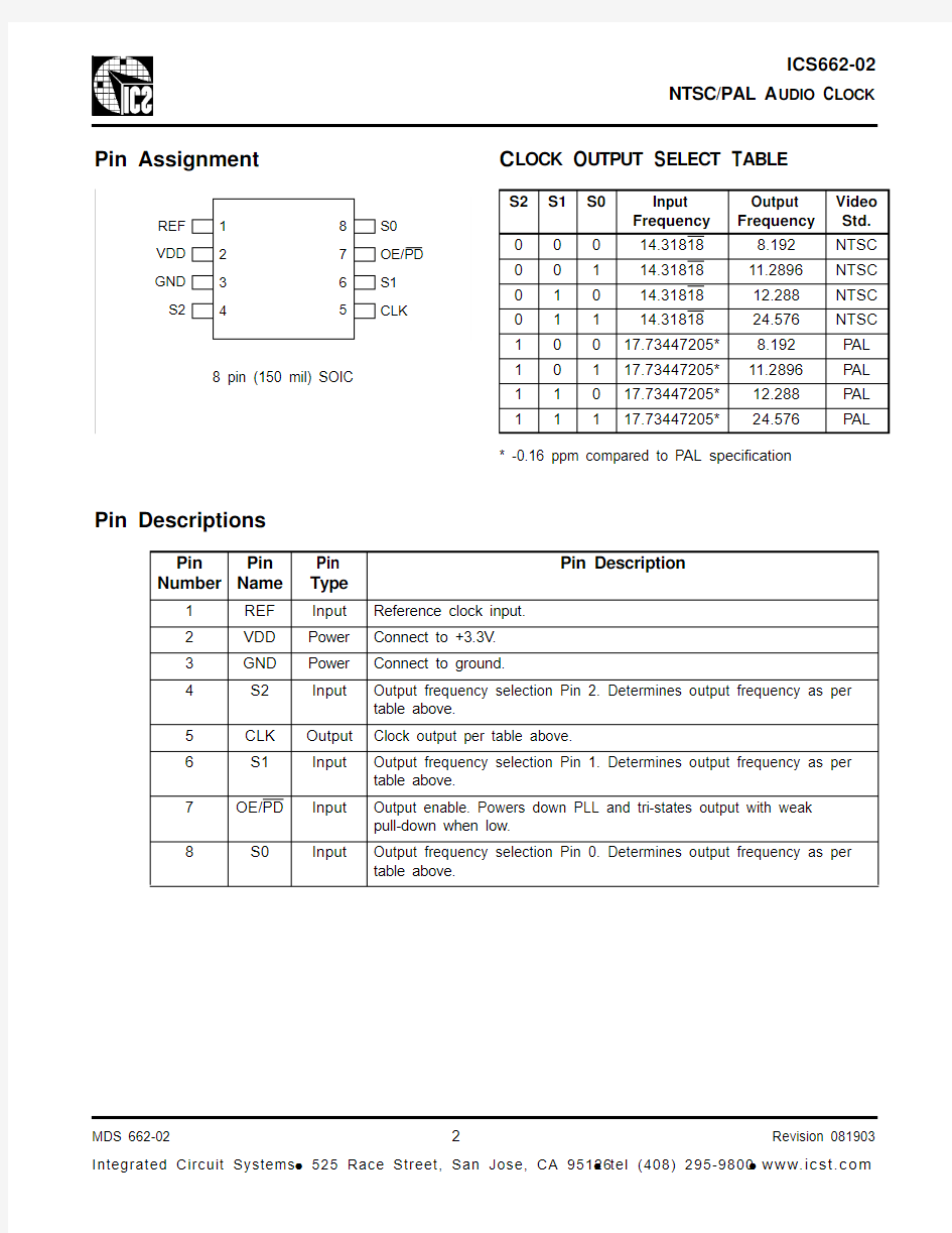
Pin Assignment
C LOCK O UTPUT S ELECT T ABLE
* -0.16 ppm compared to P AL specification Pin Descriptions
Pin Number
Pin
Name
Pin
Type
Pin Description
1REF Input Reference clock input.
2VDD Power Connect to +3.3V.
3GND Power Connect to ground.
4S2Input Output frequency selection Pin 2. Determines output frequency as per
table above.
5CLK Output Clock output per table above.
6S1Input Output frequency selection Pin 1. Determines output frequency as per
table above.
7OE/PD Input Output enable. Powers down PLL and tri-states output with weak
pull-down when low.
8S0Input Output frequency selection Pin 0. Determines output frequency as per
table above.
External Components
Decoupling Capacitor
As with any high performance mixed-signal IC, the ICS662-02 must be isolated from system power supply noise to perform optimally.
A decoupling capacitor of 0.01μF must be connected between VDD and GND on pins 2 and 3. It must be connected close to the ICS662-02 to minimize lead
inductance. No external power supply filtering is required for the ICS662-02.
Series Termination Resistor
A 33? terminating resistor can be used next to the clock outputs for trace lengths over one inch.
Absolute Maximum Ratings
Stresses above the ratings listed below can cause permanent damage to the ICS662-02. These ratings, which are standard values for ICS commercially rated parts, are stress ratings only. Functional operation of the device at these or any other conditions above those indicated in the operational sections of the
specifications is not implied. Exposure to absolute maximum rating conditions for extended periods can affect product reliability. Electrical parameters are guaranteed only over the recommended operating temperature range.
Recommended Operation Conditions
Item
Rating
Supply Voltage, VDD -0.5V to 4V
All Inputs and Outputs
-0.5V to VDD+0.5V Ambient Operating T emperature 0 to +70°C Storage T emperature -65 to +150°C Soldering T emperature
260°C
Parameter
Min.
Typ.Max.
Units
Ambient Operating T emperature
0+70°C
Power Supply Voltage (measured in respect to GND)
+3.0
+3.6
V
DC Electrical Characteristics
VDD=3.3V ±10% , Ambient temperature 0 to +70°C, unless stated otherwise
AC Electrical Characteristics
VDD = 3.3V ±10%, Ambient Temperature 0 to +70° C, unless stated otherwise
Parameter
Symbol
Conditions
Min.
Typ.
Max.
Units
Operating Voltage VDD 3.0
3.6
V Supply Current
IDD
No Load, OE/PD=1, first 4 modes 20
mA
No Load, OE/PD=1, last 4 modes 25mA
No load, OE/PDTS=0
15μA
Input High Voltage V IH OE/PD pin only VDD - 0.5V Input Low Voltage V IL OE/PD pin only 0.5
V Input High Voltage V IH S2:S0, REF pins 2.0
V Input Low Voltage V IL S2:S0, REF pins 0.8V Output High Voltage V OH I OH = -12 mA 2.4
V Output Low Voltage
V OL I OL = 12 mA 0.4
V Output High Voltage, CMOS level V OH I OH = -4 mA VDD-0.4
V Operating Supply Current IDD No load,last 4 modes 25mA Short Circuit Current I OS CLK outputs
+50mA Input Capacitance
C IN 5pF
Nominal Output Impedance Z Out 20
?
Internal pull-up resistor
R PU
S2 pin 510k ?S1, S0 OE/PD pins
120k ?Internal pull-down resistor
R PD
CLK pin
240
k ?
Parameter
Symbol
Conditions
Min.
Typ.Max.
Units
Input Crystal or Clock Frequency F IN
1020MHz Frequency Synthesis Error NTSC Clocks 0ppm P AL Clocks -0.16
ppm Output Clock Rise Time
t OR
20% to 80%, Note 1
1.5
ns
Note 1: Measured with 15 pF load.
Thermal Characteristics
Output Clock Fall Time t OF
80% to 20%, Note 1 1.5ns Output Clock Duty Cycle at VDD/2, Note 1
45
55
%Maximum Absolute Jitter, short term
Deviation from mean, Note 1
±100ps Maximum Absolute Jitter, long term Deviation from mean, Note 1, 10 μs delay
±400
ps
Parameter
Symbol
Conditions
Min.Typ.
Max.Units
Thermal Resistance Junction to Ambient
θJA Still air 150°C/W θJA 1 m/s air flow 140°C/W θJA 3 m/s air flow
120°C/W Thermal Resistance Junction to Case
θJC
40
°C/W
Parameter
Symbol
Conditions
Min.
Typ.Max.
Units
Package Outline and Package Dimensions (8 pin SOIC, 150 Mil. Narrow Body)
Package dimensions are kept current with JEDEC Publication No. 95
Ordering Information
While the information presented herein has been checked for both accuracy and reliability, Integrated Circuit Systems (ICS) assumes no responsibility for either its use or for the infringement of any patents or other rights of third parties, which would result from its use. No other circuits, patents, or licenses are implied. This product is intended for use in normal commercial applications. Any other applications such as those requiring extended temperature range, high reliability, or other extraordinary environmental requirements are not recommended without additional processing by ICS. ICS reserves the right to change any circuitry or specifications without notice. ICS does not authorize or warrant any ICS product for use in life support devices or critical medical instruments.
Part / Order Number
(Note 1)
Marking
Shipping packaging
Package
Temperature
ICS662M-02662M-02T ubes 8 pin SOIC 0 to +70° C ICS662M-02TR
662M-02
T ape and Reel
8 pin SOIC
0 to +70° C