LPC2132FHN64中文资料

1.General description
The LPC2131/32/34/36/38 microcontrollers are based on a 16/32-bit ARM7TDMI-S CPU with real-time emulation and embedded trace support, that combine the microcontroller with 32kB, 64kB, 128kB, 256kB and 512 kB of embedded high-speed ?ash memory. A 128-bit wide memory interface and a unique accelerator architecture enable 32-bit code execution at maximum clock rate.For critical code size applications,the alternative 16-bit Thumb mode reduces code by more than 30% with minimal performance penalty.Due to their tiny size and low power consumption, these microcontrollers are ideal for applications where miniaturization is a key requirement, such as access control and point-of-sale. With a wide range of serial communications interfaces and on-chip SRAM options of 8kB, 16kB, and 32kB, they are very well suited for communication gateways and protocol converters, soft modems, voice recognition and low-end imaging, providing both large buffer size and high processing power. Various 32-bit timers, single or dual 10-bit 8-channel ADC(s), 10-bit DAC, PWM channels and 47 GPIO lines with up to nine edge or level sensitive external interrupt pins make these microcontrollers particularly suitable for industrial control and medical systems.
2.Features
2.1Enhancements brought by LPC213x/01 devices
I Fast GPIO ports enable port pin toggling up to 3.5 times faster than the original LPC213x. They also allow for a port pin to be read at any time regardless of its function.
I Dedicated result registers for ADC(s) reduce interrupt overhead.
I UART0/1 include fractional baud rate generator, auto-bauding capabilities and handshake ?ow-control fully implemented in hardware.
I Additional BOD control enables further reduction of power consumption.
2.2Key features common for LPC213x and LPC213x/01
I 16/32-bit ARM7TDMI-S microcontroller in a tiny LQFP64 or HVQFN package.
I 8/16/32kB of on-chip static RAM and 32/64/128/256/512kB of on-chip ?ash program memory. 128-bit wide interface/accelerator enables high-speed 60MHz operation.I In-System Programming/In-Application Programming (ISP/IAP)via on-chip bootloader software.Single ?ash sector or full chip erase in 400ms and programming of 256B in 1 ms.
I EmbeddedICE RT and Embedded T race interfaces offer real-time debugging with the on-chip RealMonitor software and high-speed tracing of instruction execution.
LPC2131/32/34/36/38
Single-chip 16/32-bit microcontrollers; 32/64/128/256/512kB ISP/IAP ?ash with 10-bit ADC and DAC
Rev. 04 — 16 October 2007
Product data sheet
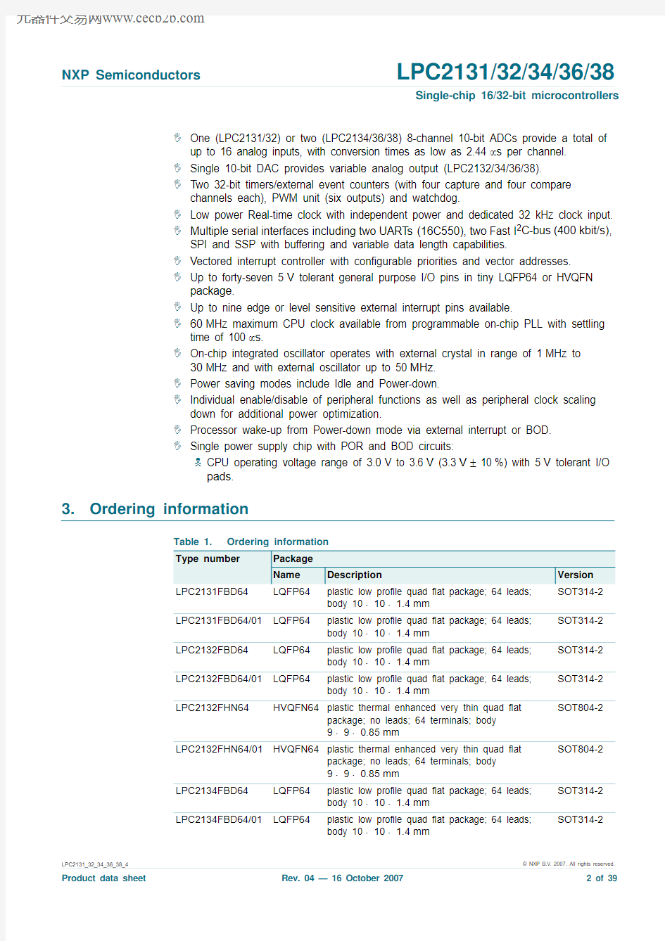
I One (LPC2131/32) or two (LPC2134/36/38) 8-channel 10-bit ADCs provide a total of
up to 16 analog inputs, with conversion times as low as 2.44μs per channel.
I Single 10-bit DAC provides variable analog output (LPC2132/34/36/38).
I T wo 32-bit timers/external event counters (with four capture and four compare
channels each), PWM unit (six outputs) and watchdog.
I Low power Real-time clock with independent power and dedicated 32 kHz clock input.
I Multiple serial interfaces including two UARTs(16C550),two Fast I2C-bus(400kbit/s),
SPI and SSP with buffering and variable data length capabilities.
I Vectored interrupt controller with con?gurable priorities and vector addresses.
I Up to forty-seven 5V tolerant general purpose I/O pins in tiny LQFP64 or HVQFN
package.
I Up to nine edge or level sensitive external interrupt pins available.
I60MHz maximum CPU clock available from programmable on-chip PLL with settling time of 100μs.
I On-chip integrated oscillator operates with external crystal in range of 1MHz to
30MHz and with external oscillator up to 50MHz.
I Power saving modes include Idle and Power-down.
I Individual enable/disable of peripheral functions as well as peripheral clock scaling
down for additional power optimization.
I Processor wake-up from Power-down mode via external interrupt or BOD.
I Single power supply chip with POR and BOD circuits:
N CPU operating voltage range of 3.0V to 3.6V (3.3V± 10%) with 5V tolerant I/O
pads.
3.Ordering information
Table 1.Ordering information
Type number Package
Name Description Version LPC2131FBD64LQFP64plastic low pro?le quad ?at package; 64 leads;
SOT314-2
body 10×10×1.4mm
SOT314-2 LPC2131FBD64/01LQFP64plastic low pro?le quad ?at package; 64 leads;
body 10×10×1.4mm
SOT314-2 LPC2132FBD64LQFP64plastic low pro?le quad ?at package; 64 leads;
body 10×10×1.4mm
LPC2132FBD64/01LQFP64plastic low pro?le quad ?at package; 64 leads;
SOT314-2
body 10×10×1.4mm
SOT804-2 LPC2132FHN64HVQFN64plastic thermal enhanced very thin quad ?at
package; no leads; 64 terminals; body
9×9×0.85mm
SOT804-2 LPC2132FHN64/01HVQFN64plastic thermal enhanced very thin quad ?at
package; no leads; 64 terminals; body
9×9×0.85mm
SOT314-2 LPC2134FBD64LQFP64plastic low pro?le quad ?at package; 64 leads;
body 10×10×1.4mm
LPC2134FBD64/01LQFP64plastic low pro?le quad ?at package; 64 leads;
SOT314-2
body 10×10×1.4mm
3.1Ordering options
LPC2136FBD64LQFP64plastic low pro?le quad ?at package; 64 leads;body 10×10×1.4mm
SOT314-2LPC2136FBD64/01LQFP64plastic low pro?le quad ?at package; 64 leads;body 10×10×1.4mm
SOT314-2LPC2138FBD64LQFP64plastic low pro?le quad ?at package; 64 leads;body 10× 10×1.4mm
SOT314-2LPC2138FBD64/01LQFP64
plastic low pro?le quad ?at package; 64 leads;body 10× 10×1.4mm
SOT314-2LPC2138FHN64
HVQFN64plastic thermal enhanced very thin quad ?at
package; no leads; 64 terminals; body 9×9×0.85mm
SOT804-2
LPC2138FHN64/01HVQFN64plastic thermal enhanced very thin quad ?at
package; no leads; 64 terminals; body 9×9×0.85mm
SOT804-2
Table 1.
Ordering information …continued
Type number Package Name
Description
Version Table 2.
Ordering options
Type number
Flash memory RAM ADC
DAC
Enhanced UARTs,ADC,Fast I/Os,and BOD
Temperature range LPC2131FBD6432kB 8kB 1-no ?40°C to +85°C LPC2131FBD64/0132kB 8kB
1
-yes ?40°C to +85°C LPC2132FBD6464kB 16kB 11no ?40°C to +85°C LPC2132FBD64/0164kB 16kB 11yes ?40°C to +85°C LPC2132FHN6464kB 16kB 11no ?40°C to +85°C LPC2132FHN64/0164kB 16kB 11yes ?40°C to +85°C LPC2134FBD64128kB 16kB 21no ?40°C to +85°C LPC2134FBD64/01128kB 16kB 21yes ?40°C to +85°C LPC2136FBD64256kB 32kB 21no ?40°C to +85°C LPC2136FBD64/01256kB 32kB 21yes ?40°C to +85°C LPC2138FBD64512kB 32kB 21no ?40°C to +85°C LPC2138FBD64/01512kB 32kB 21yes ?40°C to +85°C LPC2138FHN64512kB 32kB 21no ?40°C to +85°C LPC2138FHN64/01
512kB
32kB 2
1
yes
?40°C to +85°C
4.Block diagram
(1)LPC2134/36/38 only.(2)LPC2132/34/36/38 only.(3)Pins shared with GPIO.
Fig 1.Block diagram
SCL0,1P0[31:0]P1[31:16]
P0[31:0]P1[31:16]
SDA0,1XTAL2
XTAL1
SCK0,1MOSI0,1MISO0,1EINT[3:0]
AD0[7:0]PWM[6:1]SSEL0,1TXD0,1RXD0,1
AHB BRIDGE
PLL
UART0/UART1
REAL TIME CLOCK
PWM0
ARM7TDMI-S
RESET LPC2131, LPC2131/01LPC2132, LPC2132/01LPC2134, LPC2134/01LPC2136, LPC2136/01LPC2138, LPC2138/01
8 × CAP 8 × MAT AD1[7:0](1)
AOUT (2)DSR1(1),CTS1(1)RTS1(1), DTR1(1)DCD1(1), RI1(1)002aab067
TRST (3)
TMS (3)
TCK (3)
TDI (3)
TDO (3)trace
signals
FAST GENERAL PURPOSE I/O
INTERNAL SRAM CONTROLLER
INTERNAL FLASH CONTROLLER
8/16/32 kB SRAM
32/64/128/256/512 kB FLASH
EXTERNAL INTERRUPTS
CAPTURE/COMPARE TIMER 0/TIMER 1
A/D CONVERTERS
0 AND 1(1)
D/A CONVERTER (2)
GENERAL PURPOSE I/O
SYSTEM CONTROL
WATCHDOG TIMER
RTCX2RTCX1
SPI AND SSP SERIAL INTERFACES
I 2C SERIAL
INTERFACES 0 AND 1
APB (ARM peripheral bus)
AHB TO APB BRIDGE
APB DIVIDER
AHB DECODER
AMBA AHB
(Advanced High-performance Bus)
VECTORED INTERRUPT CONTROLLER
SYSTEM FUNCTIONS system clock
E M U L A T I O N
T R A C E M O D U L E
TEST/DEBUG INTERFACE
ARM7 local bus
VBAT
5.Pinning information
5.1Pinning
Fig 2.LPC2131 LQFP64 pinning
LPC2131LPC2131/01
P0.21/PWM5/CAP1.3P1.20/TRACESYNC P0.22/CAP0.0/MAT0.0
P0.17/CAP1.2/SCK1/MAT1.2RTCX1
P0.16/EINT0/MAT0.2/CAP0.2P1.19/TRACEPKT3
P0.15/EINT2RTCX2P1.21/PIPESTAT0V SS V DD V DDA
V SS
P1.18/TRACEPKT2
P0.14/EINT1/SDA1P0.25/AD0.4
P1.22/PIPESTAT1P0.26/AD0.5P0.13/MAT1.1P0.27/AD0.0/CAP0.1/MAT0.1P0.12/MAT1.0P1.17/TRACEPKT1P0.11/CAP1.1/SCL1P0.28/AD0.1/CAP0.2/MAT0.2P1.23/PIPESTAT2P0.29/AD0.2/CAP0.3/MAT0.3P0.10/CAP1.0
P0.30/AD0.3/EINT3/CAP0.0P0.9/RXD1/PWM6/EINT3P1.16/TRACEPKT0P0.8/TXD1/PWM4
P 0.31P 1.27/T D O
V S S V R E F
P 0.0/T X D 0/P W M 1X T A L 1
P 1.31/T R S T X T A L 2
P 0.1/R X D 0/P W M 3/E I N T 0P 1.28/T D I
P 0.2/S C L 0/C A P 0.0V S S A
V D D P 0.23
P 1.26/R T C K R E S E T
V S S P 1.29/T C K
P 0.3/S D A 0/M A T 0.0/E I N T 1P 0.20/M A T 1.3/S S E L 1/E I N T 3
P 0.4/S C K 0/C A P 0.1/A D 0.6P 0.19/M A T 1.2/M O S I 1/C A P 1.2
P 1.25/E X T I N 0P 0.18/C A P 1.3/M I S O 1/M A T 1.3
P 0.5/M I S O 0/M A T 0.1/A D 0.7P 1.30/T M S
P 0.6/M O S I 0/C A P 0.2V D D
P 0.7/S S E L 0/P W M 2/E I N T 2V S S
P 1.24/T R A C E C L K V B A T
002aab068
123456789
10
11
12
131415
16
4847464544434241403938373635343317
18
19
20
21
22
23
24
25
26
27
28
29
30
31
32
64636261605958575655545352515049
Fig 3.LPC2132 LQFP64 pin con?guration
LPC2132LPC2132/01
P0.21/PWM5/CAP1.3P1.20/TRACESYNC P0.22/CAP0.0/MAT0.0
P0.17/CAP1.2/SCK1/MAT1.2RTCX1
P0.16/EINT0/MAT0.2/CAP0.2P1.19/TRACEPKT3
P0.15/EINT2RTCX2P1.21/PIPESTAT0V SS V DD V DDA
V SS
P1.18/TRACEPKT2P0.14/EINT1/SDA1P0.25/AD0.4/AOUT
P1.22/PIPESTAT1P0.26/AD0.5P0.13/MAT1.1P0.27/AD0.0/CAP0.1/MAT0.1P0.12/MAT1.0P1.17/TRACEPKT1P0.11/CAP1.1/SCL1P0.28/AD0.1/CAP0.2/MAT0.2P1.23/PIPESTAT2P0.29/AD0.2/CAP0.3/MAT0.3P0.10/CAP1.0
P0.30/AD0.3/EINT3/CAP0.0P0.9/RXD1/PWM6/EINT3P1.16/TRACEPKT0P0.8/TXD1/PWM4
P 0.31P 1.27/T D O
V S S V R E F
P 0.0/T X D 0/P W M 1X T A L 1
P 1.31/T R S T X T A L 2
P 0.1/R X D 0/P W M 3/E I N T 0P 1.28/T D I
P 0.2/S C L 0/C A P 0.0V S S A
V D D P 0.23
P 1.26/R T C K R E S E T
V S S P 1.29/T C K
P 0.3/S D A 0/M A T 0.0/E I N T 1P 0.20/M A T 1.3/S S E L 1/E I N T 3
P 0.4/S C K 0/C A P 0.1/A D 0.6P 0.19/M A T 1.2/M O S I 1/C A P 1.2
P 1.25/E X T I N 0P 0.18/C A P 1.3/M I S O 1/M A T 1.3
P 0.5/M I S O 0/M A T 0.1/A D 0.7P 1.30/T M S
P 0.6/M O S I 0/C A P 0.2V D D
P 0.7/S S E L 0/P W M 2/E I N T 2V S S
P 1.24/T R A C E C L K V B A T
002aab406
123456789
10
11
12
131415
16
4847464544434241403938373635343317
18
19
20
21
22
23
24
25
26
27
28
29
30
31
32
64636261605958575655545352515049
Fig 4.LPC2134/36/38 LQFP64 pin con?guration
LPC2134, LPC2134/01LPC2136, LPC2136/01LPC2138, LPC2138/01
P0.21/PWM5/AD1.6/CAP1.3P1.20/TRACESYNC P0.22/AD1.7/CAP0.0/MAT0.0
P0.17/CAP1.2/SCK1/MAT1.2RTCX1
P0.16/EINT0/MAT0.2/CAP0.2P1.19/TRACEPKT3
P0.15/RI1/EINT2/AD1.5RTCX2P1.21/PIPESTAT0V SS V DD V DDA
V SS
P1.18/TRACEPKT2P0.14/DCD1/EINT1/SDA1P0.25/AD0.4/AOUT
P1.22/PIPESTAT1
P0.26/AD0.5P0.13/DTR1/MAT1.1/AD1.4P0.27/AD0.0/CAP0.1/MAT0.1P0.12/DSR1/MAT1.0/AD1.3P1.17/TRACEPKT1P0.11/CTS1/CAP1.1/SCL1P0.28/AD0.1/CAP0.2/MAT0.2P1.23/PIPESTAT2P0.29/AD0.2/CAP0.3/MAT0.3P0.10/RTS1/CAP1.0/AD1.2P0.30/AD0.3/EINT3/CAP0.0P0.9/RXD1/PWM6/EINT3P1.16/TRACEPKT0P0.8/TXD1/PWM4/AD1.1
P 0.31P 1.27/T D O
V S S V R E F
P 0.0/T X D 0/P W M 1X T A L 1
P 1.31/T R S T X T A L 2
P 0.1/R X D 0/P W M 3/E I N T 0P 1.28/T D I
P 0.2/S C L 0/C A P 0.0V S S A
V D D P 0.23
P 1.26/R T C K R E S E T
V S S P 1.29/T C K
P 0.3/S D A 0/M A T 0.0/E I N T 1P 0.20/M A T 1.3/S S E L 1/E I N T 3
P 0.4/S C K 0/C A P 0.1/A D 0.6P 0.19/M A T 1.2/M O S I 1/C A P 1.2
P 1.25/E X T I N 0P 0.18/C A P 1.3/M I S O 1/M A T 1.3
P 0.5/M I S O 0/M A T 0.1/A D 0.7P 1.30/T M S
P 0.6/M O S I 0/C A P 0.2/A D 1.0V D D
P 0.7/S S E L 0/P W M 2/E I N T 2V S S
P 1.24/T R A C E C L K V B A T
002aab407
123456789
10
11
12
131415
16
4847464544434241403938373635343317
18
19
20
21
22
23
24
25
26
27
28
29
30
31
32
64636261605958575655545352515049
AD1.7 to AD1.0 only available on LPC2134/36/38.
Fig 5.LPC2132/38 HVQFN64 pin con?guration
002aab943
LPC2132/2138
T ransparent top view
16
3315
341435133612
3711
3810
399
408417426435444453462471486463626160595857565554535251504917
18
19
20
21
22
23
24
25
26
27
28
29
30
31
32
terminal 1index area
P0.21/PWM5/AD1.6/CAP1.3P0.22/AD1.7/CAP0.0/MAT0.0
RTCX1
P1.19/TRACEPKT3
RTCX2V SS V DDA
P1.18/TRACEPKT2P0.25/AD0.4/AOUT
P0.26/AD0.5P0.27/AD0.0/CAP0.1/MAT0.1P1.17/TRACEPKT1P0.28/AD0.1/CAP0.2/MAT0.2P0.29/AD0.2/CAP0.3/MAT0.3P0.30/AD0.3/EINT3/CAP0.0P1.16/TRACEPKT0P 1.27/T D O
V R E F
X T A L 1
X T A L 2
P 1.28/T D I
V S S A
P 0.23
R E S E T
P 1.29/T C K
P 0.20/M A T 1.3/S S E L 1/E I N T 3
P 0.19/M A T 1.2/M O S I 1/C A P 1.2
P 0.18/C A P 1.3/M I S O 1/M A T 1.3
P 1.30/T M S
V D D
V S S
V B A T
P1.20/TRACESYNC P0.17/CAP1.2/SCK1/MAT1.2P0.16/EINT0/MAT0.2/CAP0.2P0.15/RI1/EINT2/AD1.5P1.21/PIPESTAT0V DD V SS
P0.14/DCD1/EINT1/SDA1P1.22/PIPESTAT1
P0.13/DTR1/MAT1.1/AD1.4P0.12/DSR1/MAT1.0/AD1.3P0.11/CTS1/CAP1.1/SCL1P1.23/PIPESTAT2P0.10/RTS1/CAP1.0/AD1.2P0.9/RXD1/PWM6/EINT3P0.8/TXD1/PWM4/AD1.1
P 0.31V S S P 0.0/T X D 0/P W M 1P 1.31/T R S T P 0.1/R X D 0/P W M 3/E I N T 0P 0.2/S C L 0/C A P 0.0V D D P 1.26/R T C K V S S P 0.3/S D A 0/M A T 0.0/E I N T 1P 0.4/S C K 0/C A P 0.1/A D 0.6P 1.25/E X T I N 0P 0.5/M I S O 0/M A T 0.1/A D 0.7P 0.6/M O S I 0/C A P 0.2/A D 1.0P 0.7/S S E L 0/P W M 2/E I N T 2P 1.24/T R A C E C L K
5.2Pin description
Table 3.Pin description
Symbol Pin Type Description
P0.0 to P0.31I/O Port0:Port0is a32-bit I/O port with individual direction controls for each bit.
T otal of 31 pins of the Port 0 can be used as a general purpose bidirectional
digital I/Os while P0.31 is output only pin. The operation of port 0 pins
depends upon the pin function selected via the pin connect block.
Pin P0.24 is not available.
P0.0/TXD0/ PWM119[1]O TXD0 —Transmitter output for UART0.
O PWM1 —Pulse Width Modulator output 1.
P0.1/RXD0/ PWM3/EINT021[2]I RXD0 —Receiver input for UART0.
O PWM3 —Pulse Width Modulator output 3.
I EINT0 —External interrupt 0 input.
P0.2/SCL0/ CAP0.022[3]I/O SCL0 —I2C0 clock input/output. Open drain output (for I2C-bus compliance).
I CAP0.0 —Capture input for Timer0, channel 0.
P0.3/SDA0/ MA T0.0/EINT126[3]I/O SDA0 —I2C0 data input/output. Open drain output (for I2C-bus compliance).
O MAT0.0 —Match output for Timer0, channel 0.
I EINT1 —External interrupt 1 input.
P0.4/SCK0/ CAP0.1/AD0.627[4]I/O SCK0 —Serial clock for SPI0.SPI clock output from master or input to slave.
I CAP0.1 —Capture input for Timer0, channel 1.
I AD0.6 —ADC 0, input 6. This analog input is always connected to its pin.
P0.5/MISO0/ MA T0.1/AD0.729[4]I/O MISO0 —Master In Slave V DD = 3.6 V for SPI0. Data input to SPI master or
data output from SPI slave.
O MAT0.1 —Match output for Timer0, channel 1.
I AD0.7 —ADC 0, input 7. This analog input is always connected to its pin.
P0.6/MOSI0/ CAP0.2/AD1.030[4]I/O MOSI0 —Master Out Slave In for SPI0.Data output from SPI master or data
input to SPI slave.
I CAP0.2 —Capture input for Timer0, channel 2.
I AD1.0 —ADC 1, input 0. This analog input is always connected to its pin.
Available in LPC2134/36/38 only.
P0.7/SSEL0/ PWM2/EINT231[2]I SSEL0 —Slave Select for SPI0. Selects the SPI interface as a slave.
O PWM2 —Pulse Width Modulator output 2.
I EINT2 —External interrupt 2 input.
P0.8/TXD1/ PWM4/AD1.133[4]O TXD1 —Transmitter output for UART1.
O PWM4 —Pulse Width Modulator output 4.
I AD1.1 —ADC 1, input 1. This analog input is always connected to its pin.
Available in LPC2134/36/38 only.
P0.9/RXD1/ PWM6/EINT334[2]I RXD1 —Receiver input for UART1.
O PWM6 —Pulse Width Modulator output 6.
I EINT3 —External interrupt 3 input.
P0.10/RTS1/ CAP1.0/AD1.235[4]O RTS1 —Request to Send output for UART1. Available in LPC2134/36/38.
I CAP1.0 —Capture input for Timer1, channel 0.
I AD1.2 —ADC 1, input 2. This analog input is always connected to its pin.
Available in LPC2134/36/38 only.
P0.11/CTS1/ CAP1.1/SCL137[3]I CTS1 —Clear to Send input for UART1. Available in LPC2134/36/38.
I CAP1.1 —Capture input for Timer1, channel 1.
I/O SCL1 —I2C1 clock input/output. Open drain output (for I2C-bus compliance)
P0.12/DSR1/ MA T1.0/AD1.338[4]I DSR1 —Data Set Ready input for UART1. Available in LPC2134/36/38.
O MAT1.0 —Match output for Timer1, channel 0.
I AD1.3 —ADC 1, input 3. This analog input is always connected to its pin.
Available in LPC2134/36/38 only.
P0.13/DTR1/ MA T1.1/AD1.439[4]O DTR1 —Data Terminal Ready output for UART1. Available in
LPC2134/36/38.
O MAT1.1 —Match output for Timer1, channel 1.
I AD1.4 —ADC 1, input 4. This analog input is always connected to its pin.
Available in LPC2134/36/38 only.
P0.14/DCD1/ EINT1/SDA141[3]I DCD1 —Data Carrier Detect input for UART1. Available in LPC2134/36/38.
I EINT1 —External interrupt 1 input.
I/O SDA1 —I2C1 data input/output. Open drain output (for I2C-bus compliance).
P0.15/RI1/ EINT2/AD1.545[4]I RI1 —Ring Indicator input for UART1. Available in LPC2134/36/38.
I EINT2 —External interrupt 2 input.
I AD1.5 —ADC 1, input 5. This analog input is always connected to its pin.
Available in LPC2134/36/38 only.
P0.16/EINT0/ MA T0.2/CAP0.246[2]I EINT0 —External interrupt 0 input.
O MAT0.2 —Match output for Timer0, channel 2.
I CAP0.2 —Capture input for Timer0, channel 2.
P0.17/CAP1.2/ SCK1/MA T1.247[1]I CAP1.2 —Capture input for Timer1, channel 2.
I/O SCK1 —Serial Clock for SSP. Clock output from master or input to slave.
O MAT1.2 —Match output for Timer1, channel 2.
P0.18/CAP1.3/ MISO1/MA T1.353[1]I CAP1.3 —Capture input for Timer1, channel 3.
I/O MISO1 —Master In Slave Out for SSP. Data input to SPI master or data
output from SSP slave.
O MAT1.3 —Match output for Timer1, channel 3.
P0.19/MA T1.2/ MOSI1/CAP1.254[1]O MAT1.2 —Match output for Timer1, channel 2.
I/O MOSI1 —Master Out Slave In for SSP.Data output from SSP master or data
input to SSP slave.
I CAP1.2 —Capture input for Timer1, channel 2.
P0.20/MA T1.3/ SSEL1/EINT355[2]O MAT1.3 —Match output for Timer1, channel 3.
I SSEL1 —Slave Select for SSP. Selects the SSP interface as a slave.
I EINT3 —External interrupt 3 input.
P0.21/PWM5/ AD1.6/CAP1.31[4]O PWM5 —Pulse Width Modulator output 5.
I AD1.6 —ADC 1, input 6. This analog input is always connected to its pin.
Available in LPC2134/36/38 only.
I CAP1.3 —Capture input for Timer1, channel 3.
Table 3.Pin description …continued
Symbol Pin Type Description
P0.22/AD1.7/ CAP0.0/MA T0.02[4]I AD1.7 —ADC 1, input 7. This analog input is always connected to its pin.
Available in LPC2134/36/38 only.
I CAP0.0 —Capture input for Timer0, channel 0.
O MAT0.0 —Match output for Timer0, channel 0.
P0.2358[1]I/O General purpose digital input/output pin.
P0.25/AD0.4/ AOUT 9[5]I AD0.4 —ADC 0, input 4. This analog input is always connected to its pin.
O AOUT —DAC output. Not available in LPC2131.
P0.26/AD0.510[4]I AD0.5 —ADC 0, input 5. This analog input is always connected to its pin.
P0.27/AD0.0/ CAP0.1/MA T0.111[4]I AD0.0 —ADC 0, input 0. This analog input is always connected to its pin.
I CAP0.1 —Capture input for Timer0, channel 1.
O MAT0.1 —Match output for Timer0, channel 1.
P0.28/AD0.1/ CAP0.2/MA T0.213[4]I AD0.1 —ADC 0, input 1. This analog input is always connected to its pin.
I CAP0.2 —Capture input for Timer0, channel 2.
O MAT0.2 —Match output for Timer0, channel 2.
P0.29/AD0.2/ CAP0.3/MA T0.314[4]I AD0.2 —ADC 0, input 2. This analog input is always connected to its pin.
I CAP0.3 —Capture input for Timer0, channel 3.
O MAT0.3 —Match output for Timer0, channel 3.
P0.30/AD0.3/ EINT3/CAP0.015[4]I AD0.3 —ADC 0, input 3. This analog input is always connected to its pin.
I EINT3 —External interrupt 3 input.
I CAP0.0 —Capture input for Timer0, channel 0.
P0.3117[6]O General purpose digital output only pin.
Important: This pin MUST NOT be externally pulled LOW when RESET pin
is LOW or the JTAG port will be disabled.
P1.0 to P1.31I/O Port1:Port1is a32-bit bidirectional I/O port with individual direction controls
for each bit. The operation of port 1 pins depends upon the pin function
selected via the pin connect block. Pins 0 through 15 of port1 are not
available.
P1.16/
TRACEPKT0
16[6]O TRACEPKT0 —T race Packet, bit 0. Standard I/O port with internal pull-up.
P1.17/
TRACEPKT1
12[6]O TRACEPKT1 —T race Packet, bit 1. Standard I/O port with internal pull-up.
P1.18/
TRACEPKT2
8[6]O TRACEPKT2 —T race Packet, bit 2. Standard I/O port with internal pull-up.
P1.19/
TRACEPKT3
4[6]O TRACEPKT3 —T race Packet, bit 3. Standard I/O port with internal pull-up.
P1.20/ TRACESYNC 48[6]O TRACESYNC —Trace Synchronization. Standard I/O port with internal
pull-up. LOW on TRACESYNC while RESET is LOW enables pins P1.25:16
to operate as Trace port after reset.
P1.21/
PIPEST A T0
44[6]O PIPESTAT0 —Pipeline Status, bit 0. Standard I/O port with internal pull-up.
P1.22/
PIPEST A T1
40[6]O PIPESTAT1 —Pipeline Status, bit 1. Standard I/O port with internal pull-up.
P1.23/ PIPEST A T236[6]O PIPESTAT2 —Pipeline Status, bit 2. Standard I/O port with internal pull-up.
Table 3.Pin description …continued
Symbol Pin Type Description
[1]5V tolerant pad providing digital I/O functions with TTL levels and hysteresis and 10ns slew rate control.
[2]5V tolerant pad providing digital I/O functions with TTL levels and hysteresis and 10ns slew rate control. If con?gured for an input function, this pad utilizes built-in glitch ?lter that blocks pulses shorter than 3 ns.
[3]Open drain 5V tolerant digital I/O I 2C-bus 400kHz speci?cation compatible pad. It requires external pull-up to provide an output functionality.
[4]
5V tolerant pad providing digital I/O (with TTL levels and hysteresis and 10ns slew rate control)and analog input function.If con?gured for an input function, this pad utilizes built-in glitch ?lter that blocks pulses shorter than 3 ns. When con?gured as an ADC input, digital section of the pad is disabled.
[5]5V tolerant pad providing digital I/O (with TTL levels and hysteresis and 10ns slew rate control) and analog output function. When con?gured as the DAC output, digital section of the pad is disabled.
[6]5V tolerant pad with built-in pull-up resistor providing digital I/O functions with TTL levels and hysteresis and 10ns slew rate control.The pull-up resistor’s value ranges from 60 k ? to 300 k ?.
[7]5V tolerant pad providing digital input (with TTL levels and hysteresis) function only.[8]
Pad provides special analog functionality.
P1.24/
TRACECLK 32[6]O TRACECLK —Trace Clock. Standard I/O port with internal pull-up.P1.25/EXTIN028[6]I EXTIN0 —External T rigger Input. Standard I/O with internal pull-up.P1.26/RTCK
24[6]
I/O
RTCK —Returned Test Clock output. Extra signal added to the JT AG port.Assists debugger synchronization when processor frequency varies.
Bidirectional pin with internal pull-up. LOW on RTCK while RESET is LOW enables pins P1.31:26 to operate as Debug port after reset.P1.27/TDO 64[6]O TDO —Test Data out for JTAG interface.P1.28/TDI 60[6]I TDI —Test Data in for JTAG interface.P1.29/TCK 56[6]I TCK —Test Clock for JTAG interface.P1.30/TMS 52[6]I TMS —Test Mode Select for JTAG interface.P1.31/TRST 20[6]I TRST —Test Reset for JTAG interface.
RESET
57[7]
I
External reset input:A LOW on this pin resets the device,causing I/O ports and peripherals to take on their default states, and processor execution to begin at address 0. TTL with hysteresis, 5V tolerant.
XT AL162[8]I Input to the oscillator circuit and internal clock generator circuits.XT AL261[8]O Output from the oscillator ampli?er.RTCX13[8]I Input to the RTC oscillator circuit.RTCX25[8]
O
Output from the RTC oscillator circuit.V SS 6,18,25,42,50I Ground: 0V reference.
V SSA 59I Analog ground: 0V reference. This should nominally be the same voltage as V SS , but should be isolated to minimize noise and error.
V DD 23, 43, 51I 3.3V power supply: This is the power supply voltage for the core and I/O ports.
V DDA
7
I
Analog 3.3V power supply: This should be nominally the same voltage as V DD but should be isolated to minimize noise and error. This voltage is used to power the on-chip PLL.
VREF 63I
ADC reference: This should be nominally the same voltage as V DD but
should be isolated to minimize noise and error. Level on this pin is used as a reference for A/D and D/A convertor(s).
VBAT
49I
RTC power supply: 3.3 V on this pin supplies the power to the RTC.
Table 3.Pin description …continued
Symbol
Pin Type Description
6.Functional description
6.1Architectural overview
The ARM7TDMI-S is a general purpose 32-bit microprocessor, which offers high
performance and very low power consumption. The ARM architecture is based on
Reduced Instruction Set Computer (RISC) principles, and the instruction set and related
decode mechanism are much simpler than those of microprogrammed Complex
Instruction Set Computers. This simplicity results in a high instruction throughput and
impressive real-time interrupt response from a small and cost-effective processor core.
Pipeline techniques are employed so that all parts of the processing and memory systems
can operate continuously. Typically, while one instruction is being executed, its successor
is being decoded, and a third instruction is being fetched from memory.
The ARM7TDMI-S processor also employs a unique architectural strategy known as
Thumb, which makes it ideally suited to high-volume applications with memory
restrictions, or applications where code density is an issue.
The key idea behind Thumb is that of a super-reduced instruction set. Essentially, the
ARM7TDMI-S processor has two instruction sets:
?The standard 32-bit ARM set.
? A 16-bit Thumb set.
The Thumb set’s 16-bit instruction length allows it to approach twice the density of
standard ARM code while retaining most of the ARM’s performance advantage over a
traditional 16-bit processor using 16-bit registers. This is possible because Thumb code
operates on the same 32-bit register set as ARM code.
Thumb code is able to provide up to 65% of the code size of ARM, and 160% of the
performance of an equivalent ARM processor connected to a 16-bit memory system.
6.2On-chip ?ash program memory
The LPC2131/32/34/36/38 incorporate a 32kB, 64kB, 128kB, 256kB and 512kB ?ash
memory system respectively. This memory may be used for both code and data storage.
Programming of the ?ash memory may be accomplished in several ways. It may be
programmed In System via the serial port.The application program may also erase and/or
program the ?ash while the application is running, allowing a great degree of ?exibility for
data storage ?eld ?rmware upgrades, etc. When the LPC2131/32/34/36/38 on-chip
bootloader is used, 32/64/128/256/500kB of ?ash memory is available for user code.
The LPC2131/32/34/36/38 ?ash memory provides a minimum of 100000 erase/write
cycles and 20 years of data-retention.
6.3On-chip static RAM
On-chip static RAM may be used for code and/or data storage. The SRAM may be
accessed as 8-bit, 16-bit, and 32-bit. The LPC2131, LPC2132/34, and LPC2136/38
provide 8kB, 16kB and 32kB of static RAM respectively.
6.4Memory map
The LPC2131/32/34/36/38 memory map incorporates several distinct regions, as shown in Figure 6.
In addition, the CPU interrupt vectors may be re-mapped to allow them to reside in either ?ash memory (the default) or on-chip static RAM. This is described in Section 6.18“System control”.
Fig 6.LPC2131/32/34/36/38 memory map
AHB PERIPHERALS
VPB PERIPHERALS
RESERVED ADDRESS SPACE
RESERVED ADDRESS SPACE
BOOT BLOCK (RE-MAPPED FROM
ON-CHIP FLASH MEMORY RESERVED ADDRESS SPACE
TOTAL OF 32 kB ON-CHIP STA TIC RAM (LPC2136/38)TOTAL OF 16 kB ON-CHIP STA TIC RAM (LPC2132/34)TOTAL OF 8 kB ON-CHIP STATIC RAM (LPC2131)
TOTAL OF 512 kB ON-CHIP NON-VOLA TILE MEMORY
(LPC2138)TOTAL OF 256 kB ON-CHIP NON-VOLA TILE MEMORY
(LPC2136)TOTAL OF 128 kB ON-CHIP NON-VOLA TILE MEMORY
(LPC2134)0xFFFF FFFF 0xF000 00000xE000 0000
0xC000 0000
0x8000 0000
0x4000 40000x4000 3FFF 0x4000 20000x4000 1FFF 0x4001 80000x4000 7FFF
0x4000 0000
0x0004 00000x0003 FFFF 0x0002 00000x0001 FFFF 0x0008 00000x0007 FFFF 0x0001 00004.0 GB
3.75 GB
3.5 GB
3.0 GB
2.0 GB
1.0 GB
TOTAL OF 64 kB ON-CHIP NON-VOLATILE MEMORY
(LPC2132)TOTAL OF 32 kB ON-CHIP NON-VOLATILE MEMORY
(LPC2131)
0x0000 FFFF 0x0000 80000x0000 7FFF 0x0000 0000
0.0 GB
002aab069
6.5Interrupt controller
The Vectored Interrupt Controller (VIC) accepts all of the interrupt request inputs and
categorizes them as Fast Interrupt Request (FIQ), vectored Interrupt Request (IRQ), and non-vectored IRQ as de?ned by programmable settings. The programmable assignment scheme means that priorities of interrupts from the various peripherals can be dynamically assigned and adjusted.
FIQ has the highest priority. If more than one request is assigned to FIQ, the VIC
combines the requests to produce the FIQ signal to the ARM processor. The fastest
possible FIQ latency is achieved when only one request is classi?ed as FIQ,because then the FIQ service routine can simply start dealing with that device. But if more than one
request is assigned to the FIQ class,the FIQ service routine can read a word from the VIC that identi?es which FIQ source(s) is (are) requesting an interrupt.
Vectored IRQs have the middle priority.Sixteen of the interrupt requests can be assigned to this category. Any of the interrupt requests can be assigned to any of the 16 vectored IRQ slots, among which slot 0 has the highest priority and slot 15 has the lowest.
Non-vectored IRQs have the lowest priority.
The VIC combines the requests from all the vectored and non-vectored IRQs to produce the IRQ signal to the ARM processor. The IRQ service routine can start by reading a
register from the VIC and jumping there. If any of the vectored IRQs are requesting, the VIC provides the address of the highest-priority requesting IRQs service routine,
otherwise it provides the address of a default routine that is shared by all the non-vectored IRQs. The default routine can read another VIC register to see what IRQs are active. 6.5.1Interrupt sources
Table4lists the interrupt sources for each peripheral function.Each peripheral device has one interrupt line connected to the Vectored Interrupt Controller, but may have several
internal interrupt ?ags. Individual interrupt ?ags may also represent more than one
interrupt source.
Table 4.Interrupt sources
Block Flag(s)VIC channel #
WDT Watchdog Interrupt (WDINT)0
-Reserved for software interrupts only1
ARM Core EmbeddedICE, DbgCommRX2
ARM Core EmbeddedICE, DbgCommTX3
TIMER0Match 0 to 3 (MR0, MR1, MR2, MR3)
4
Capture 0 to 3 (CR0, CR1, CR2, CR3)
5 TIMER1Match 0 to 3 (MR0, MR1, MR2, MR3)
Capture 0 to 3 (CR0, CR1, CR2, CR3)
UART0RX Line Status (RLS)
6
T ransmit Holding Register empty (THRE)
RX Data Available (RDA)
Character Time-out Indicator (CTI)
6.6Pin connect block
The pin connect block allows selected pins of the microcontroller to have more than one function. Con?guration registers control the multiplexers to allow connection between the pin and the on chip peripherals. Peripherals should be connected to the appropriate pins prior to being activated,and prior to any related interrupt(s)being enabled.Activity of any enabled peripheral function that is not mapped to a related pin should be considered unde?ned.
6.7General purpose parallel I/O and Fast I/O
Device pins that are not connected to a speci?c peripheral function are controlled by the GPIO registers. Pins may be dynamically con?gured as inputs or outputs. Separate
registers allow setting or clearing any number of outputs simultaneously.The value of the output register may be read back, as well as the current state of the port pins.
6.7.1Features
?Direction control of individual bits.
?Separate control of output set and clear.?All I/O default to inputs after reset.
UART1
RX Line Status (RLS)
T ransmit Holding Register empty (THRE)RX Data Available (RDA)
Character Time-out Indicator (CTI)
Modem Status Interrupt (MSI) (Available in LPC2134/36/38only)
7
PWM0Match 0 to 6 (MR0, MR1, MR2, MR3, MR4, MR5, MR6)Capture 0 to 3 (CR0, CR1, CR2, CR3)8I 2C0SI (state change)9SPI0SPIF , MODF
10SSP
TX FIFO at least half empty (TXRIS)RX FIFO at least half full (RXRIS)Receive Timeout (RTRIS)Receive Overrun (RORRIS)
11
PLL PLL Lock (PLOCK)
12RTC
RTCCIF (Counter Increment), RTCALF (Alarm)13System Control
External Interrupt 0 (EINT0)14External Interrupt 1 (EINT1)15External Interrupt 2 (EINT2)16External Interrupt 3 (EINT3)
17AD0ADC 0
18I2C1SI (state change)19BOD Brown Out Detect
20AD1
ADC 1 (Available in LPC2134/36/38 only)
21
Table 4.Interrupt sources …continued
Block Flag(s)
VIC channel #
6.7.2Fast I/O features available in LPC213x/01 only
?Fast I/O registers are located on the ARM local bus for the fastest possible I/O timing.
?All GPIO registers are byte addressable.
?Entire port value can be written in one instruction.
?Mask registers allow single instruction to set or clear any number of bits in one port.
6.810-bit ADC
The LPC2131/32 contain one and the LPC2134/36/38 contain two ADCs. These
converters are single 10-bit successive approximation ADCs with eight multiplexed
channels.
6.8.1Features
?Measurement range of 0V to 3.3V.
?Each converter capable of performing more than 400000 10-bit samples per second.
?Burst conversion mode for single or multiple inputs.
?Optional conversion on transition on input pin or Timer Match signal.
?Global Start command for both converters (LPC2134/36/38 only).
6.8.2ADC features available in LPC213x/01 only
?Every analog input has a dedicated result register to reduce interrupt overhead.
?Every analog input can generate an interrupt once the conversion is completed.
6.910-bit DAC
This peripheral is available in the LPC2132/34/36/38 only. The DAC enables the
LPC2132/34/36/38 to generate variable analog output.
6.9.1Features
?10-bit digital to analog converter.
?Buffered output.
?Power-down mode available.
?Selectable speed versus power.
6.10UARTs
The LPC2131/32/34/36/38 each contain two UARTs. In addition to standard transmit and
receive data lines, the LPC2134/36/38 UART1 also provides a full modem control
handshake interface.
6.10.1Features
?16B Receive and T ransmit FIFOs.
?Register locations conform to 16C550 industry standard.
?Receiver FIFO trigger points at 1B, 4B, 8B, and 14B
?Built-in baud rate generator.
?Standard modem interface signals included on UART1. (LPC2134/36/38 only)
?The LPC2131/32/34/36/38 transmission FIFO control enables implementation of software (XON/XOFF) ?ow control on both UARTs and hardware (CTS/RTS) ?ow
control on the LPC2134/36/38 UART1 only.
6.10.2UART features available in LPC213x/01 only
?Fractional baud rate generator enables standard baud rates such as 115200 to be achieved with any crystal frequency above 2 MHz.
?Auto-bauding.
?Auto-CTS/RTS ?ow-control fully implemented in hardware (LPC2134/36/38 only).
6.11I2C-bus serial I/O controller
The LPC2131/32/34/36/38 each contain two I2C-bus controllers.
The I2C-bus is bidirectional, for inter-IC control using only two wires: a serial clock line
(SCL), and a serial data line (SDA). Each device is recognized by a unique address and
can operate as either a receiver-only device (e.g., an LCD driver or a transmitter with the capability to both receive and send information (such as memory)). Transmitters and/or
receivers can operate in either master or slave mode,depending on whether the chip has to initiate a data transfer or is only addressed.The I2C-bus is a multi-master bus,it can be controlled by more than one bus master connected to it.
This I2C-bus implementation supports bit rates up to 400kbit/s (Fast I2C).
6.11.1Features
?Standard I2C compliant bus interface.
?Easy to con?gure as Master, Slave, or Master/Slave.
?Programmable clocks allow versatile rate control.
?Bidirectional data transfer between masters and slaves.
?Multi-master bus (no central master).
?Arbitration between simultaneously transmitting masters without corruption of serial data on the bus.
?Serial clock synchronization allows devices with different bit rates to communicate via one serial bus.
?Serial clock synchronization can be used as a handshake mechanism to suspend and resume serial transfer.
?The I2C-bus may be used for test and diagnostic purposes.
6.12SPI serial I/O controller
The LPC2131/32/34/36/38each contain one SPI controller.The SPI is a full duplex serial interface,designed to be able to handle multiple masters and slaves connected to a given bus. Only a single master and a single slave can communicate on the interface during a
given data transfer. During a data transfer the master always sends a byte of data to the
slave, and the slave always sends a byte of data to the master.
6.12.1Features
?Compliant with Serial Peripheral Interface (SPI) speci?cation.
?Synchronous, Serial, Full Duplex, Communication.
?Combined SPI master and slave.
?Maximum data bit rate of one eighth of the input clock rate.
6.13SSP serial I/O controller
The LPC2131/32/34/36/38 each contain one Serial Synchronous Port controller (SSP).
The SSP controller is capable of operation on a SPI, 4-wire SSI, or Microwire bus. It can
interact with multiple masters and slaves on the bus.However,only a single master and a single slave can communicate on the bus during a given data transfer.The SSP supports full duplex transfers, with frames of 4 bits to 16 bits of data ?owing from the master to the slave and from the slave to the master. Often only one of these data ?ows carries
meaningful data.
6.13.1Features
?Compatible with Motorola SPI, 4-wire TI SSI and National Semiconductor Microwire buses.
?Synchronous Serial Communication.
?Master or slave operation.
?8-frame FIFOs for both transmit and receive.
?Four bits to 16 bits per frame.
6.14General purpose timers/external event counters
The Timer/Counter is designed to count cycles of the peripheral clock (PCLK) or an
externally supplied clock, and optionally generate interrupts or perform other actions at
speci?ed timer values, based on four match registers. It also includes four capture inputs to trap the timer value when an input signal transitions,optionally generating an interrupt.
Multiple pins can be selected to perform a single capture or match function, providing an
application with ‘or’ and ‘and’, as well as ‘broadcast’ functions among them.
At any given time only one of peripheral’s capture inputs can be selected as an external
event signal source,i.e.,timer’s clock.The rate of external events that can be successfully counted is limited to PCLK/2. In this con?guration, unused capture lines can be selected
as regular timer capture inputs.
6.14.1Features
? A 32-bit Timer/Counter with a programmable 32-bit Prescaler.
?External Event Counter or timer operation.
?Four 32-bit capture channels per timer/counter that can take a snapshot of the timer value when an input signal transitions. A capture event may also optionally generate
an interrupt.
?Four 32-bit match registers that allow:
–Continuous operation with optional interrupt generation on match.
–Stop timer on match with optional interrupt generation.
–Reset timer on match with optional interrupt generation.
?Four external outputs per timer/counter corresponding to match registers, with the following capabilities:
–Set LOW on match.
–Set HIGH on match.
–Toggle on match.
–Do nothing on match.
6.15Watchdog timer
The purpose of the watchdog is to reset the microcontroller within a reasonable amount of time if it enters an erroneous state. When enabled, the watchdog will generate a system
reset if the user program fails to ‘feed’ (or reload) the watchdog within a predetermined
amount of time.
6.15.1Features
?Internally resets chip if not periodically reloaded.
?Debug mode.
?Enabled by software but requires a hardware reset or a watchdog reset/interrupt to be disabled.
?Incorrect/Incomplete feed sequence causes reset/interrupt if enabled.
?Flag to indicate watchdog reset.
?Programmable 32-bit timer with internal pre-scaler.
?Selectable time period from(T cy(PCLK)×256×4)to(T cy(PCLK)×232×4)in multiples of
T cy(PCLK)×4.
6.16Real-time clock
The Real-Time Clock (RTC) is designed to provide a set of counters to measure time
when normal or idle operating mode is selected.The RTC has been designed to use little power, making it suitable for battery powered systems where the CPU is not running
continuously (Idle mode).
6.16.1Features
?Measures the passage of time to maintain a calendar and clock.
?Ultra-low power design to support battery powered systems.
?Provides Seconds,Minutes,Hours,Day of Month,Month,Y ear,Day of Week,and Day of Y ear.
?Can use either the RTC dedicated 32 kHz oscillator input or clock derived from the external crystal/oscillator input at XTAL1. Programmable Reference Clock Divider
allows ?ne adjustment of the RTC.
?Dedicated power supply pin can be connected to a battery or the main 3.3V.