tlv5619

FEATURES DESCRIPTION
APPLICATIONS
D2
D3
D4
D5
D6
D7
D8
D9
D10
D11
DW OR PW PACKAGE
(TOP VIEW)
TLV5619
SLAS172F–DECEMBER1997–REVISED FEBRUARY2004
2.7V TO5.5V12-BIT PARALLEL DIGITAL-TO-ANALOG CONVERTER
WITH POWER DOWN
?Single Supply2.7-V to5.5-V Operation The TLV5619is a12-bit voltage output DAC with a
microprocessor and TMS320compatible parallel ?±0.4LSB Differential Nonlinearity(DNL),
interface.The12data bits are double buffered so that ±1.5LSB Integral Nonlinearity(INL)
the output can be updated asynchronously using the ?12-Bit Parallel Interface
LDAC pin.During normal operation,the device dissi-?Compatible With TMS320DSP pates8mW at a5-V supply and4.3mW at a3-V
supply.The power consumption can be lowered to50?Internal Power On Reset
nW by setting the DAC to power-down mode.?Settling Time1μs Typ
The output voltage is buffered by a×2gain
rail-to-rail ?Low Power Consumption:
amplifier,which features a Class A output stage to –8mW for5-V Supply
improve stability and reduce settling time.
–4.3mW for3-V Supply
?Reference Input Buffers
?Voltage Output
?Monotonic Over Temperature
?Asynchronous Update
?Battery Powered Test Instruments
?Digital Offset and Gain Adjustment
?Battery Operated/Remote Industrial Controls
?Machine and Motion Control Devices
?Cordless and Wireless Telephones
?Speech Synthesis
AVAILABLE OPTIONS ?Communication Modulators
?Arbitrary Waveform Generation
Please be aware that an important notice concerning availability,standard warranty,and use in critical applications of Texas
Instruments semiconductor products and disclaimers thereto appears at the end of this data sheet.
https://www.wendangku.net/doc/da18587161.html,
OUT TLV5619
SLAS172F–DECEMBER1997–REVISED FEBRUARY2004
These devices have limited built-in ESD protection.The leads should be shorted together or the device placed in conductive foam during storage or handling to prevent electrostatic damage to the MOS gates.
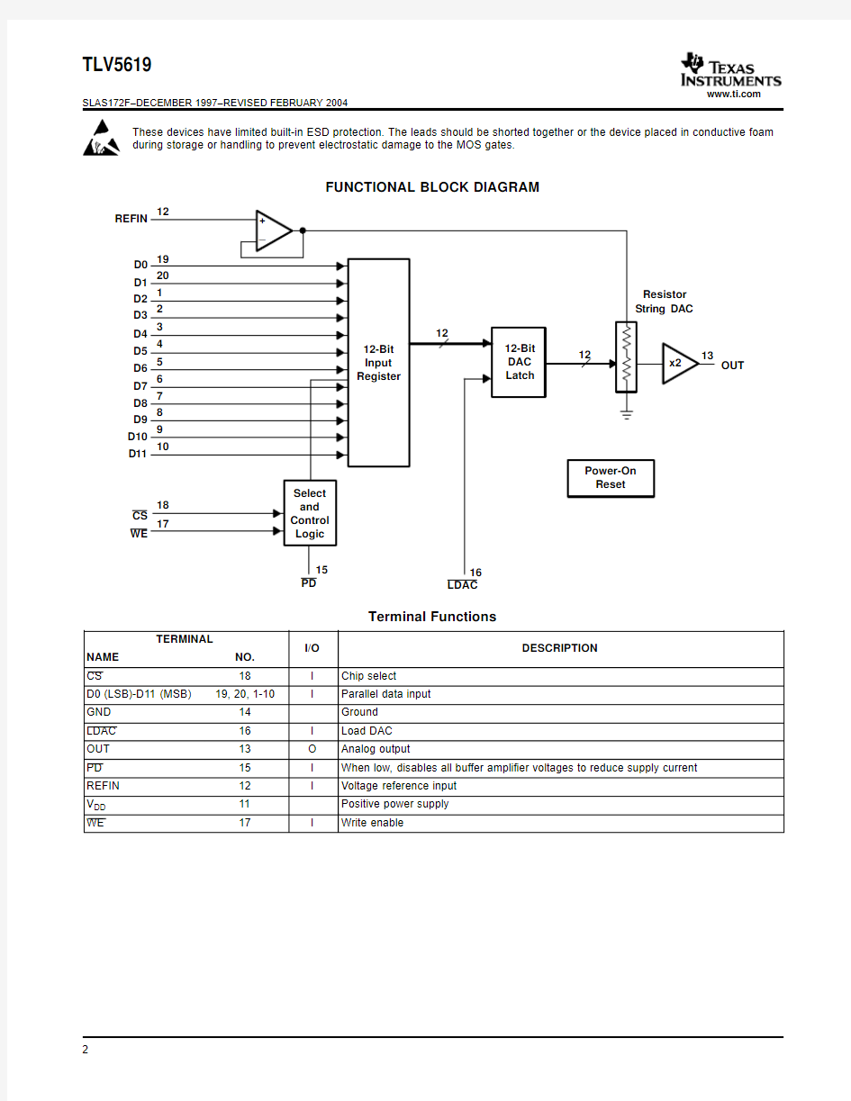
FUNCTIONAL BLOCK DIAGRAM
Terminal Functions
https://www.wendangku.net/doc/da18587161.html,
ABSOLUTE MAXIMUM RATINGS RECOMMENDED OPERATING CONDITIONS
TLV5619 SLAS172F–DECEMBER1997–REVISED FEBRUARY2004
over operating free-air temperature range(unless otherwise noted)(1)
(1)Stresses beyond those listed under,,absolute maximum ratings”may cause permanent damage to the device.These are stress ratings
only,and functional operation of the device at these or any other conditions beyond those indicated under,,recommended operating conditions”is not implied.Exposure to absolute-maximum-rated conditions for extended periods may affect device reliability.
https://www.wendangku.net/doc/da18587161.html, ELECTRICAL CHARACTERISTICS
TLV5619
SLAS172F–DECEMBER 1997–REVISED FEBRUARY 2004over recommended operating free-air temperature range,sdupply voltages,and reference voltages (unless otherwise noted)
(1)The relative accuracy or integral nonlinearity (INL),sometimes referred to as linearity error,is the maximum deviation of the output from
the line between zero and full scale excluding the effects of zero code and full-scale errors.
(2)The differential nonlinearity (DNL),sometimes referred to as differential error,is the difference between the measured and ideal 1LSB
amplitude change of any two adjacent codes.Monotonic means the output voltage changes in the same direction (or remains constant)as a change in the digital input code.
(3)Zero-scale error is the deviation from zero voltage output when the digital input code is zero.
(4)Zero-scale-error temperature coefficient is given by:E
ZS TC =[E ZS (T max )-E ZS (T min )]/V ref ×106/(T max -T min ).
(5)Gain error is the deviation from the ideal output (2×V ref -1LSB)with an output load of 10k ?excluding the effects of the zero-error.
(6)Gain temperature coefficient is given by:E G TC =[E G (T max )-E G (T min )]/V ref ×106/(T max -T min ).
(7)Zero-scale-error rejection ratio (EZS-RR)is measured by varying the V DD from 4.5V to 5.5V dc and measuring the proportion of this
signal imposed on the zero-code output voltage.
(8)Gain-error rejection ratio (EG-RR)is measured by varying the V DD from 4.5V to 5.5V dc and measuring the proportion of this signal
https://www.wendangku.net/doc/da18587161.html, TIMING REQUIREMENTS
TLV5619
SLAS172F–DECEMBER 1997–REVISED FEBRUARY 2004
(1)
Reference input voltages greater than V DD /2will cause output saturation for large DAC codes.
(2)Reference feedthrough is measured at the DAC output with an input code =0x000and a V ref(REFIN)input =1.024V dc +1V pp at
(1)
Settling time is the time for the output signal to remain within ±0.5LSB of the final measured value for a digital input code change of 32to 4063or 4063to 32.Limits are ensured by design and characterization,but are not production tested.(2)1kHz sinewave generated by DAC,reference voltage =1.024V at 3V and 2.048V at 5V.
https://www.wendangku.net/doc/da18587161.html,
PARAMETER MEASUREMENT INFORMATION
D(0–11)CS
WE
LDAC
TLV5619
SLAS172F–DECEMBER 1997–REVISED FEBRUARY 2004Figure 1.Timing Diagram
https://www.wendangku.net/doc/da18587161.html, TYPICAL CHARACTERISTICS
321
– O u t p u t V o l t a g e – V 4
MAXIMUM OUTPUT VOLTAGE
vs
LOAD
5R L – Output Load – ?V O 21.51
0.5100 k 10 k 1 k – O u t p u t V o l t a g e – V
2.5
MAXIMUM OUTPUT VOLTAGE vs LOAD 310010
R L – Output Load – ?V O –60–80
–100
T H D – T o t a l H a r
m o n i c D i s t o r t i o n – d B –40–20TOTAL HARMONIC DISTORTION
vs
LOAD
100 k 10 k 1 k 100
10R L – Output Load – ?
f – Frequency – kHz
TOTAL HARMONIC DISTORTION vs FREQUENCY T H D – T o t a l H a r m o n i c D i s t o r t i o n – d B TLV5619
SLAS172F–DECEMBER 1997–REVISED FEBRUARY 2004
Figure 2.Figure 3.
Figure 4.Figure 5.
https://www.wendangku.net/doc/da18587161.html, 4030100
05101520S N R D – S i g n a l -T o -N o i s e R a t i o + D i s t o r t i o n – d B 5070 f – Frequency – kHz
SIGNAL-TO-NOISE + DISTORTION
vs
FREQUENCY
80
253035
60
2010.80.60.40.20-0.2-0.4-0.6-0.8-1D N L - D i f f e r e n t i a l N o n l i n e a r i t y - L S B 0500100015002000
2500300035004095Code 21.5
1
0.5
0-0.5
-1
-1.5
-2
0500100015002000
2500300035004095Code I N L - I n t e g r a l N o n l i n e a r i t y - L S B
3
4
-3
-4
TLV5619
SLAS172F–DECEMBER 1997–REVISED FEBRUARY 2004TYPICAL CHARACTERISTICS (continued)
Figure 6.
Figure 7.Differential Nonlinearity
Figure 8.Integral Nonlinearity
https://www.wendangku.net/doc/da18587161.html, POWER DOWN SUPPLY CURRENT
vs
TIME 0.00001
0.000001
100300t – Time – ms
0.010.0010.0001
20040050000.1
1600
I D D – S u p p l y C u r r e n t – m A TLV5619
SLAS172F–DECEMBER 1997–REVISED FEBRUARY 2004TYPICAL CHARACTERISTICS (continued)
Figure 9.
https://www.wendangku.net/doc/da18587161.html,
APPLICATION INFORMATION
DEFINITIONS OF SPECIFICATIONS AND TERMINOLOGY
Integral Nonlinearity (INL)
Differential Nonlinearity (DNL)
Zero-Scale Error (E ZS )
Gain Error (E G )
Signal-to-Noise Ratio +Distortion (S/N+D)
Spurious Free Dynamic Range (SFDR)
Total Harmonic Distortion (THD)
TLV5619
SLAS172F–DECEMBER 1997–REVISED FEBRUARY 2004The relative accuracy or integral nonlinearity (INL),sometimes referred to as linearity error,is the maximum deviation of the output from the line between zero and full scale excluding the effects of zero code and full-scale errors.
The differential nonlinearity (DNL),sometimes referred to as differential error,is the difference between the measured and ideal 1LSB amplitude change of any two adjacent codes.Monotonic means the output voltage changes in the same direction (or remains constant)as a change in the digital input code.
Zero-scale error is defined as the deviation of the output from 0V at a digital input value of 0.
Gain error is the error in slope of the DAC transfer function.
S/N+D is the ratio of the rms value of the output signal to the rms sum of all other spectral components below the Nyquist frequency,including harmonics but excluding dc.The value for S/N+D is expressed in decibels.
SFDR is the difference between the rms value of the output signal and the rms value of the largest spurious signal within a specified bandwidth.The value for SFDR is expressed in decibels.
THD is the ratio of the rms sum of the first six harmonic components to the rms value of the fundamental signal and is expressed in decibels.
https://www.wendangku.net/doc/da18587161.html,
LINEARITY,OFFSET,AND GAIN ERROR SUING SINGLE END SUPPLIES
Output
Voltage
0 V
Negative
Offset
GENERAL FUNCTION
2REF CODE
0x1000[V]
TLV5619 SLAS172F–DECEMBER1997–REVISED FEBRUARY2004
APPLICATION INFORMATION(continued)
When an amplifier is operated from a single supply,the voltage offset can still be either positive or negative.With a positive offset,the output voltage changes on the first code change.With a negative offset the output voltage may not change with the first code depending on the magnitude of the offset voltage.
The output amplifier attempts to drive the output to a negative voltage.However,because the most negative supply rail is ground,the output cannot drive below ground and clamps the output at0V.
The output voltage remains at zero until the input code value produces a sufficient positive output voltage to overcome the negative offset voltage,resulting in the transfer function shown in Figure10.
Figure10.Effect of Negative Offset(Single Supply)
This offset error,not the linearity error,produces this breakpoint.The transfer function would have followed the dotted line if the output buffer could drive below the ground rail.
For a DAC,linearity is measured between zero input code(all inputs0)and full scale code(all inputs1)after offset and full scale are adjusted out or accounted for in some way.However,single supply operation does not allow for adjustment when the offset is negative due to the breakpoint in the transfer function.So the linearity is measured between full scale code and the lowest code that produces a positive output voltage.
The TLV5619is a12-bit,single supply DAC,based on a resistor string architecture.It consists of a parallel interface,a power down control logic,a resistor string,and a rail-to-rail output buffer.The output voltage(full scale determined by reference)is given by:
Where REF is the reference voltage and CODE is the digital input value,range0x000to0xFFF.A power on reset initially puts the internal latches to a defined state(all bits zero).
https://www.wendangku.net/doc/da18587161.html, PARALLEL INTERFACE
TLV5619
SLAS172F–DECEMBER 1997–REVISED FEBRUARY 2004APPLICATION INFORMATION (continued)
The device latches data on the positive edge of WE.It must be enabled with CS low.LDAC low updates the DAC with the value in the holding latch.LDAC is an asynchronous input and can be held low,if a separate update is not necessary.However,to control the DAC using the load feature,LDAC can be driven low after the positive WE edge.
Figure 11.Proposed Interface Between TLV5619and TMS320C2XX,5X DSPs
Figure 12.Proposed Interface Between TLV5619and TMS320C3X DSPs
https://www.wendangku.net/doc/da18587161.html,
TLV5619INTERFACED TO TMS320C203DSP Hardware Interface
Software
TLV5619 SLAS172F–DECEMBER1997–REVISED FEBRUARY2004
APPLICATION INFORMATION(continued)
Figure13shows an example of the connection between the TLV5619and the TMS320C203DSP.The only other device that is needed in addition to the DSP and the DAC is the74AC138address decoding https://www.wendangku.net/doc/da18587161.html,ing this configuration,the DAC address is0x0084within the I/O memory space of the TMS320C203.
LDAC is held low so that the output voltage is updated with the rising WE edge.The power down mode is deactivated permanently by pulling PD to V DD.
Figure13.TLV5619to TMS320C203DSP Interface Connection
No setup procedure is needed to access the TLV5619.The output voltage can be set using one command:
out data_addr,DAC_addr
Where data_addr points to the address location(in this example0x0060)holding the new output voltage data and DAC_addr is the I/O space address of the TLV5619(in this example0x0084).
The following code shows,how to use the timer of the TMS320C203as a time base to generate a voltage ramp with the TLV5619.A timer interrupt is generated every205μs.The corresponding interrupt service routine increments the output code(stored at0x0060)for the DAC and writes the new code to the TLV5619.Only the12 LSBs of the data in0x0060are used by the DAC,so that the resulting period of the saw waveform is:
?t=4096×205E-6s=0.84s
https://www.wendangku.net/doc/da18587161.html, SOFTWARE LISTING
TLV5619
SLAS172F–DECEMBER 1997–REVISED FEBRUARY 2004APPLICATION INFORMATION (continued)
;File:ramp.asm
;Description:This program generates a ramp.
;-------------I/O and memory mapped regs -----------
.include "regs.asm"
TLV5619.equ 0084h
;-------------vectors -------------------------------
.ps 0h
b start
b INT1
b INT23
b TIM_ISR
*********************************************************************
*Main Program
*********************************************************************
.ps 1000h
.entry
start:
ldp
#0;set data page to 0;disable interrupts
setc
INTM ;disable maskable interrupts splk
#0ffffh,IFR splk
#0004h,IMR ;set up the timer
splk
#0000h,60h splk
#0042h,61h out
61h.PRD out
60h,TIM splk
#0c2fh,62h out
62h,TCR ;enable interrupts
clrc INTM ;enable maskable interrupts
;loop forever!
next idle ;wait for interrupt
b next
;all else fails stop here
done b done ;hang there
*********************************************************************
*Interrupt Service Routines
*********************************************************************
INT1:
ret ;do nothing and return INT23:ret ;do nothing and return
TIM_ISR:
;useful code
add #1h ;increment accumulator
sacl 60h
https://www.wendangku.net/doc/da18587161.html,
TLV5619 SLAS172F–DECEMBER1997–REVISED FEBRUARY2004
APPLICATION INFORMATION(continued)
out60h,TLV5619;write to DAC
clrc intm;re-enable interrupts
ret;return from interrupt
.end
PACKAGING INFORMATION
Orderable Device Status(1)Package
Type Package
Drawing
Pins Package
Qty
Eco Plan(2)Lead/Ball Finish MSL Peak Temp(3)
TLV5619CDW ACTIVE SOIC DW2025Green(RoHS&
no Sb/Br)
CU NIPDAU Level-1-260C-UNLIM
TLV5619CDWG4ACTIVE SOIC DW2025Green(RoHS&
no Sb/Br)
CU NIPDAU Level-1-260C-UNLIM
TLV5619CDWR ACTIVE SOIC DW202000Green(RoHS&
no Sb/Br)
CU NIPDAU Level-1-260C-UNLIM
TLV5619CDWRG4ACTIVE SOIC DW202000Green(RoHS&
no Sb/Br)
CU NIPDAU Level-1-260C-UNLIM
TLV5619CPW ACTIVE TSSOP PW2070Green(RoHS&
no Sb/Br)
CU NIPDAU Level-1-260C-UNLIM
TLV5619CPWG4ACTIVE TSSOP PW2070Green(RoHS&
no Sb/Br)
CU NIPDAU Level-1-260C-UNLIM
TLV5619CPWR ACTIVE TSSOP PW202000Green(RoHS&
no Sb/Br)
CU NIPDAU Level-1-260C-UNLIM
TLV5619CPWRG4ACTIVE TSSOP PW202000Green(RoHS&
no Sb/Br)
CU NIPDAU Level-1-260C-UNLIM
TLV5619IDW ACTIVE SOIC DW2025Green(RoHS&
no Sb/Br)
CU NIPDAU Level-1-260C-UNLIM
TLV5619IDWG4ACTIVE SOIC DW2025Green(RoHS&
no Sb/Br)
CU NIPDAU Level-1-260C-UNLIM
TLV5619IDWR ACTIVE SOIC DW202000Green(RoHS&
no Sb/Br)
CU NIPDAU Level-1-260C-UNLIM
TLV5619IDWRG4ACTIVE SOIC DW202000Green(RoHS&
no Sb/Br)
CU NIPDAU Level-1-260C-UNLIM
TLV5619IPW ACTIVE TSSOP PW2070Green(RoHS&
no Sb/Br)
CU NIPDAU Level-1-260C-UNLIM
TLV5619IPWG4ACTIVE TSSOP PW2070Green(RoHS&
no Sb/Br)
CU NIPDAU Level-1-260C-UNLIM
TLV5619IPWR ACTIVE TSSOP PW202000Green(RoHS&
no Sb/Br)
CU NIPDAU Level-1-260C-UNLIM
TLV5619IPWRG4ACTIVE TSSOP PW202000Green(RoHS&
no Sb/Br)
CU NIPDAU Level-1-260C-UNLIM TLV5619QDW ACTIVE SOIC DW2025TBD CU NIPDAU Level-1-220C-UNLIM TLV5619QDWG4ACTIVE SOIC DW2025Green(RoHS&
no Sb/Br)
CU NIPDAU Level-1-260C-UNLIM TLV5619QDWR ACTIVE SOIC DW202000TBD CU NIPDAU Level-1-220C-UNLIM TLV5619QDWRG4ACTIVE SOIC DW202000Green(RoHS&
no Sb/Br)
CU NIPDAU Level-1-260C-UNLIM
(1)The marketing status values are defined as follows:
ACTIVE:Product device recommended for new designs.
LIFEBUY:TI has announced that the device will be discontinued,and a lifetime-buy period is in effect.
NRND:Not recommended for new designs.Device is in production to support existing customers,but TI does not recommend using this part in a new design.
PREVIEW:Device has been announced but is not in production.Samples may or may not be available.
OBSOLETE:TI has discontinued the production of the device.
(2)Eco Plan-The planned eco-friendly classification:Pb-Free(RoHS),Pb-Free(RoHS Exempt),or Green(RoHS&no Sb/Br)-please check https://www.wendangku.net/doc/da18587161.html,/productcontent for the latest availability information and additional product content details.
TBD:The Pb-Free/Green conversion plan has not been defined.
Pb-Free(RoHS):TI's terms"Lead-Free"or"Pb-Free"mean semiconductor products that are compatible with the current RoHS requirements
for all6substances,including the requirement that lead not exceed0.1%by weight in homogeneous materials.Where designed to be soldered at high temperatures,TI Pb-Free products are suitable for use in specified lead-free processes.
Pb-Free(RoHS Exempt):This component has a RoHS exemption for either1)lead-based flip-chip solder bumps used between the die and package,or2)lead-based die adhesive used between the die and leadframe.The component is otherwise considered Pb-Free(RoHS compatible)as defined above.
Green(RoHS&no Sb/Br):TI defines"Green"to mean Pb-Free(RoHS compatible),and free of Bromine(Br)and Antimony(Sb)based flame retardants(Br or Sb do not exceed0.1%by weight in homogeneous material)
(3)MSL,Peak Temp.--The Moisture Sensitivity Level rating according to the JEDEC industry standard classifications,and peak solder temperature.
Important Information and Disclaimer:The information provided on this page represents TI's knowledge and belief as of the date that it is provided.TI bases its knowledge and belief on information provided by third parties,and makes no representation or warranty as to the accuracy of such information.Efforts are underway to better integrate information from third parties.TI has taken and continues to take reasonable steps to provide representative and accurate information but may not have conducted destructive testing or chemical analysis on incoming materials and chemicals.TI and TI suppliers consider certain information to be proprietary,and thus CAS numbers and other limited information may not be available for release.
In no event shall TI's liability arising out of such information exceed the total purchase price of the TI part(s)at issue in this document sold by TI to Customer on an annual basis.
OTHER QUALIFIED VERSIONS OF TLV5619:
?Enhanced Product:TLV5619-EP
NOTE:Qualified Version Definitions:
?Enhanced Product-Supports Defense,Aerospace and Medical Applications
TAPE AND REEL INFORMATION
*All dimensions are nominal Device Package Type Package Drawing
Pins
SPQ Reel Diameter (mm)Reel Width W1(mm)A0(mm)B0(mm)K0(mm)P1(mm)W (mm)Pin1Quadrant TLV5619CPWR TSSOP
PW 202000330.016.4 6.957.1 1.68.016.0Q1TLV5619IPWR TSSOP
PW 202000330.016.4 6.957.1 1.68.016.0Q1TLV5619QDWR SOIC DW 202000
330.024.410.813.0 2.712.024.0Q1
*All dimensions are nominal
Device Package Type Package Drawing Pins SPQ Length(mm)Width(mm)Height(mm) TLV5619CPWR TSSOP PW202000346.0346.033.0 TLV5619IPWR TSSOP PW202000346.0346.033.0
TLV5619QDWR SOIC DW202000346.0346.041.0