HCF4020B
s MEDIUM SPEED OPERATION:
16MHz(Typ.)at V DD=10V
s FULLY STA TIC OPERATION
s COMMON RESET
s BUFFERED INPUTS AND OUTPUTS
s STANDARDIZED SYMMETRICAL OUTPUT CHARACTERISTICS
s QUIESCENT CURRENT SPECIFIED UP TO 20V
s5V,10V AND15V PARAMETRIC RATINGS
s INPUT LEAKAGE CURRENT
I I=100nA(MAX)AT V DD=18V T A=25°C
s100%TESTED FOR QUIESCENT CURRENT s MEETS ALL REQUIREMENTS OF JEDEC JESD13B”STANDARD SPECIFICATIONS
FOR DESCRIPTION OF B SERIES CMOS
DEVICES”
DESCRIPTION
The HCF4020B is a monolithic integrated circuit fabricated in Metal Oxide Semiconductor technology available in DIP and SOP packages. The HCF4020B is a ripple carry binary counter.All counter stages are master-slave flip-flops.The state of a counter advances one count on the negative transition of each input pulse;a high level on the RESET line resets the counter to its all zeros stage.Schmitt trigger action on the input pulse line permits unlimited clock rise and fall times.
All inputs and outputs are buffered
HCF4020B
RIPPLE-CARRY BINARY COUNTER/DIVIDERS14STAGE
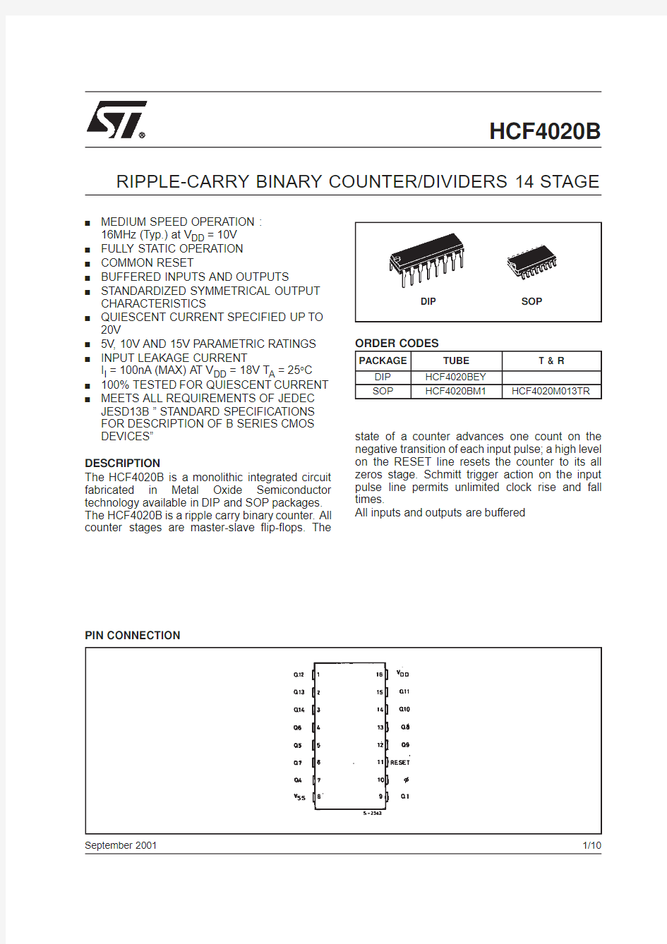
PIN CONNECTION ORDER CODES
PACKAGE TUBE T&R DIP HCF4020BEY
SOP HCF4020BM1HCF4020M013TR
DIP SOP
1/10
September2001
HCF4020B
2/10
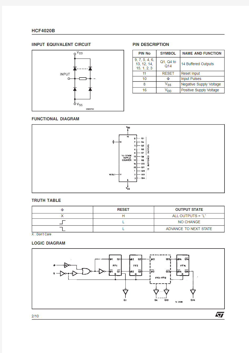
IINPUT EQUIVALENT CIRCUIT
PIN DESCRIPTION
FUNCTIONAL DIAGRAM
TRUTH TABLE
X :Don’t Care
LOGIC DIAGRAM
PIN No SYMBOL NAME AND FUNCTION 9,7,5,4,6,13,12,14,15,1,2,3
Q1,Q4to Q1414Buffered Outputs 11RESET Reset Input 10
ΦInput Pulses
8V SS Negative Supply Voltage 16
V DD
Positive Supply Voltage
ΦRESET OUTPUT STATE X
H ALL OUTPUTS =”L”
L NO CHANGE
L
ADVANCE TO NEXT STATE
HCF4020B
3/10
ABSOLUTE MAXIMUM RATINGS
Absolute Maximum Ratings are those values beyond which damage to the device may occur.Functional operation under these conditions is not implied.
All voltage values are referred to V SS pin voltage.
RECOMMENDED OPERATING CONDITIONS
Symbol Parameter
Value Unit V DD Supply Voltage -0.5to +22V V I DC Input Voltage -0.5to V DD +0.5
V I I DC Input Current
±10mA P D Power Dissipation per Package
200mW Power Dissipation per Output Transistor 100mW T op Operating Temperature -55to +125°C T stg
Storage Temperature
-65to +150
°C
Symbol Parameter
Value Unit V DD Supply Voltage 3to 20V V I Input Voltage
0to V DD V T op
Operating Temperature
-55to 125
°C
HCF4020B
4/10
DC SPECIFICATIONS
The Noise Margin for both ”1”and ”0”level is:1V min.with V DD =5V,2V min.with V DD =10V,2.5V min.with V DD =15V
Symbol
Parameter
Test Condition
Value Unit
V I (V)V O (V)
|I O |(μA)V DD (V)
T A =25°C -40to 85°C -55to 125°C Min.
Typ.Max.Min.
Max.Min.
Max.I L
Quiescent Current
0/550.045150150μA
0/10100.0410*******/15150.04206006000/20200.08
100
3000
3000
V OH
High Level Output Voltage
0/5<15 4.95 4.95 4.95V
0/10<1109.959.959.950/15<11514.95
14.95
14.95
V OL
Low Level Output Voltage 5/0<150.050.050.05V
10/0<1100.050.050.0515/0
<1150.05
0.05
0.05
V IH
High Level Input Voltage 0.5/4.5<15 3.5 3.5 3.5V
1/9<1107771.5/13.5<11511
11
11
V IL
Low Level Input Voltage 4.5/0.5<15 1.5 1.5 1.5V
9/1<11033313.5/1.5<1154
4
4
I OH
Output Drive Current
0/5 2.5<15-1.36-3.2-1.1-1.1mA
0/5 4.6<15-0.44-1-0.36-0.360/109.5<110-1.1-2.6-0.9-0.90/1513.5<115-3.0-6.8-2.4-2.4I OL
Output Sink Current
0/50.4<150.4410.360.36mA 0/100.5<110 1.1 2.60.90.90/15 1.5
<1
15 3.0
6.8 2.4
2.4
I I Input Leakage Current
0/18
Any Input 18
±10-5±0.1±1
±1
μA C I
Input Capacitance
Any Input
5
7.5
pF
HCF4020B
5/10
DYNAMIC ELECTRICAL CHARACTERISTICS (T amb =25°C,C L =50pF,R L =200K ?,t r =t f =20ns)
(*)Typical temperature coefficient for all V DD value is 0.3%/°C.
Symbol
Parameter
Test Condition
Value (*)Unit
V DD (V)
Min.
Typ.Max.INPUT-PULSE OPERATION t PLH t PHL Propagation Delay Time
(?to Q1Out)5180360ns
10801601565130t PLH t PHL Propagation Delay Time
(Qn to Qn+1)5100200ns
104080153060t THL t TLH Transition Time
5100200ns
1050100154080t W
Minimum Input Pulse Width
570140ns
103060152040
t r ,t f
Input Pulse Rise and Fall Time
5unlimited μs
1015f max
Maximum Clock Input Frequency
5 3.57MHz
1081615
12
24RESET OPERATION t PHL
Propagation Delay Time
5140280ns
10601201550100t W
Minimum Reset Pulse Width
5100200ns
104080153060t REM
Reset Removal Time
5175350ns
107515015
50
100
HCF4020B
TEST CIRCUIT
C L=50pF or equivalent(includes jig and probe capacitance)
R L=200K?
R T=Z OUT of pulse generator(typically50?)
WAVEFORM1:MINIMUM PULSE WIDTH(RESET)AND REMOVAL TIME(RESET TOΦ)(f=1MHz; 50%duty cycle)
6/10
HCF4020B WAVEFORM2:PROPAGATION DELAY TIME(f=1MHz;50%duty cycle)
WAVEFORM3:PROPAGATION DELAY TIME,MINIMUM PULSE WIDTH(Φ)(f=1MHz;50%duty cycle)
7/10
HCF4020B
8/10DIM.
mm.inch
MIN.TYP MAX.MIN.TYP.MAX. a10.510.020
B0.77 1.650.0300.065 b0.50.020
b10.250.010
D200.787 E8.50.335
e 2.540.100
e317.780.700
F7.10.280 I 5.10.201 L 3.30.130
Z 1.270.050
Plastic DIP-16(0.25)MECHANICAL DATA
P001C
HCF4020B
9/10
DIM.mm.
inch MIN.
TYP
MAX.MIN.
TYP.
MAX.A 1.750.068a10.1
0.20.0030.007a2 1.650.064b 0.350.460.0130.018b10.19
0.25
0.007
0.010
C 0.5
0.019
c145°(typ.)
D 9.8100.3850.393
E 5.8
6.2
0.228
0.244
e 1.270.050e38.89
0.350
F 3.8 4.00.1490.157
G 4.6 5.30.1810.208L 0.5 1.270.019
0.050M 0.62
0.024S
8°(max.)
SO-16MECHANICAL DATA
PO13H
HCF4020B
Information furnished is believed to be accurate and reliable.However,STMicroelectronics assumes no responsibility for the consequences of use of such information nor for any infringe ment of patents or other rights of third parties which may result from its use.No license is granted by implication or otherwise under any patent or patent rights of STMicroelectronics.Specifications mentioned in this publication are subject to change without notice.This publication supersedes and replaces all information previously supplied.STMicroelectronics products are not authorized for use as critical components in life support devices or systems without express written approval of STMicroelectronics.
?The ST logo is a registered trademark of STMicroelectronics
?2001STMicroelectronics-Printed in Italy-All Rights Reserved
STMicroelectronics GROUP OF COMPANIES
Australia-Brazil-China-Finland-France-Germany-Hong Kong-India-Italy-Japan-Malaysia-Malta-Morocco
Singapore-Spain-Sweden-Switzerland-United Kingdom
?http://w https://www.wendangku.net/doc/e84632402.html,
10/10